Semiconductor device

A technology of semiconductors and laminates, which is applied in the direction of semiconductor devices, semiconductor/solid-state device manufacturing, semiconductor/solid-state device components, etc., and can solve problems such as the limitation of independent work of multiple gate drive circuits

Inactive Publication Date: 2011-09-21
PANASONIC CORP
View PDF0 Cites 8 Cited by
  • Summary
  • Abstract
  • Description
  • Claims
  • Application Information

AI Technical Summary

Problems solved by technology

Otherwise, due to the voltage noise generated in the gate or the gate drive circuit due to the influence of parasitic inductance in the transient state, malfunction of the gate such as false detection occurs, and the effect of preventing the false detection is also suppressed.
[0015] Furthermore, in the case of configuring a plurality of gate drive circuits typified by the protection circuit, and controlling the output current of the power element with high precision or complexity, as in the drive circuit described in Patent Document 1, if As the reference potential of the protection circuit of the gate drive circuit is specified by the GND of the power line, the independent operation of multiple gate drive circuits will be limited

Method used


Image

  • Semiconductor device
  • Semiconductor device
  • Semiconductor device

Examples


Embodiment 1

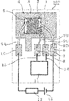
[0060] FIG. 1(a) is a top view illustrating wiring of a semiconductor device according to Embodiment 1 of the present invention. A semiconductor device 100 shown in the figure includes a semiconductor element 3 as a first semiconductor element, a plurality of bonding wires 9A to 9D as connection materials, and a gate drive circuit 11 . Furthermore, on the semiconductor device 100, the substrate terminal 4 as the first substrate terminal, the ohmic electrode terminal 6 as the first ohmic electrode terminal, the ohmic electrode terminal 10 as the second ohmic electrode terminal, and the gate driving terminal 7 , and the gate terminal 8 are arranged separately from each other, and these constitute the connection terminal portion. And, the semiconductor element 3 is bonded to the substrate terminal 4, and on the semiconductor element 3, the gate electrode pad 1, the ohmic electrode pad 2 as the first ohmic electrode pad, and the ohmic electrode pad 2 as the second ohmic electrode ...

Embodiment 2

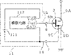
[0075] image 3 It is a circuit configuration diagram including a semiconductor device according to Embodiment 2 of the present invention. The drive system shown in this figure is a system in which a motor is driven by a single-phase inverter circuit, and the drive system includes a DC power supply 28 , a semiconductor device 110 and a motor 29 .

[0076] The semiconductor device 110 includes a half bridge 101 as a first half bridge and a half bridge 102 as a second half bridge. The half bridge 101 and the half bridge 102 have the same structure, and each has the structure of the semiconductor device 110 described in the first embodiment. That is to say, image 3 The configurations of the described semiconductor elements 3A, 3B, 3C, and 3D are the same as those of the semiconductor element 3 described in FIG. 1 . and, image 3 The structures of the described gate drive circuits 11A, 11B, 11C, and 11D are the same as those of the gate drive circuit 11 described in FIG. 1 . ...

Embodiment 3

[0083] In this embodiment, the configuration and effect of applying the present invention to a semiconductor device having a double-gate semiconductor element will be described with reference to the drawings. That is, by independently controlling the two gate electrodes arranged between the drain and the source, it is possible to control the leakage current of the semiconductor element with high precision or complexity.

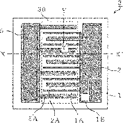
[0084] FIG. 6(a) is a top view illustrating wiring of a semiconductor device according to Embodiment 3 of the present invention. The semiconductor device 200 described in this figure includes a semiconductor element 40 as a third semiconductor element, a plurality of bonding wires 9A to 9F as connection materials, a gate drive circuit 47 as a fourth gate drive circuit, and a third connection The gate drive circuit 48 of the gate drive circuit. Furthermore, in the semiconductor device 200, the first substrate terminal 4, the ohmic electrode terminal 6 as the ...


PUM


Abstract

The present invention provides a semiconductor device which makes it possible to reduce a disturbance noise generated to the gate or the gate drive circuit of the current-driven semiconductor device by the parasitic inductance, and to increase accuracy and stability of gate drive. The semiconductor device comprises: a semiconductor element which is current driven; a gate drive circuit which controls the semiconductor element and a connection terminal unit, wherein the semiconductor element includes: a gate electrode pad formed on a stacked structure of a nitride semiconductor layer; ohmic electrodes; the said connection terminal unit includes: a first ohmic electrode terminal (6) connected to the first ohmic electrode pad; a second ohmic electrode terminal (7) connected to the second ohmic electrode pad; a gate drive terminal (7) connected to the first ohmic electrode pad; and a gate terminal (8) connected to the gate electrode pad, an input terminal of the gate drive circuit is connected to the gate drive terminal, an output terminal of the gate drive circuit is connected to the gate terminal, and a potential of the first ohmic electrode pad corresponds to a reference potential of the gate drive circuit.

Description

technical field [0001] The present invention relates to a semiconductor device for power conversion, and more particularly to a current-driven semiconductor device using a nitride semiconductor. Background technique [0002] Against the background of the global warming problem, further energy saving of electrical equipment is desired, and it is necessary to improve the power conversion efficiency of power conversion devices such as power supply circuits and inverter circuits that handle large amounts of electric power. The biggest factor that determines the power conversion efficiency of a power conversion device is the IGBT (Insulated Gate Bipolar Transistor: Insulated Gate Bipolar Transistor) or MOSFET (Metal Oxide Semiconductor Field Effect Transistor: Metal Oxide Semiconductor Field Effect Transistor) used in power conversion. Losses in power semiconductor components. If the loss in the power semiconductor element is reduced, the power conversion efficiency of the power...

Claims


Application Information

Patent Timeline
Patent Type & Authority Applications(China)
IPC IPC(8): H02M7/48H01L25/16H01L23/58H01L23/498H01L21/338H01L21/822H01L27/04H01L29/778H01L29/812H02M1/08H02M7/5387
CPCH01L2224/49112H01L2224/48472H03K3/021H01L24/06H01L2924/13091H01L2224/49171H02P6/14H01L24/49H01L2224/4903H01L2224/48247H01L2924/30107H01L2224/0603H01L2924/13055H01L2924/3011H01L2924/1306H01L2924/1305H01L2924/13062H01L2924/12032H01L2224/05553H01L2224/45014H01L2224/45124H01L2224/45147H01L2924/00014H01L24/45H01L2224/04042H01L2924/13063H01L2224/05554H01L24/48H01L2924/00H01L2224/05599H01L2924/206
Inventor 井腰文智山际优人桥诘真吾柳原学上本康裕
Owner PANASONIC CORP
Why Eureka
Try Eureka