Heterojunction field effect transistor based on channel array structure

A technology of heterojunction field effect and channel array, which is applied in the direction of semiconductor devices, electrical components, circuits, etc., and can solve the problems of very difficult process control of trench gate technology

Inactive Publication Date: 2011-09-28
SUZHOU INST OF NANO TECH & NANO BIONICS CHINESE ACEDEMY OF SCI
View PDF5 Cites 18 Cited by
  • Summary
  • Abstract
  • Description
  • Claims
  • Application Information

AI Technical Summary

Problems solved by technology

[0005] At present, the technologies for realizing enhanced HEMT devices include trench gate technology, fluorine treatment technology and the so-called GIT technology of p-type gate. The technical process control is very difficult, and the reliability of fluorine treatment technology and GIT technology has yet to be verified
In addition, based on

Method used


Image

  • Heterojunction field effect transistor based on channel array structure
  • Heterojunction field effect transistor based on channel array structure
  • Heterojunction field effect transistor based on channel array structure

Examples


Embodiment 1

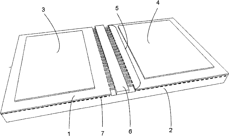
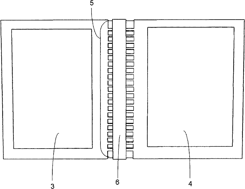
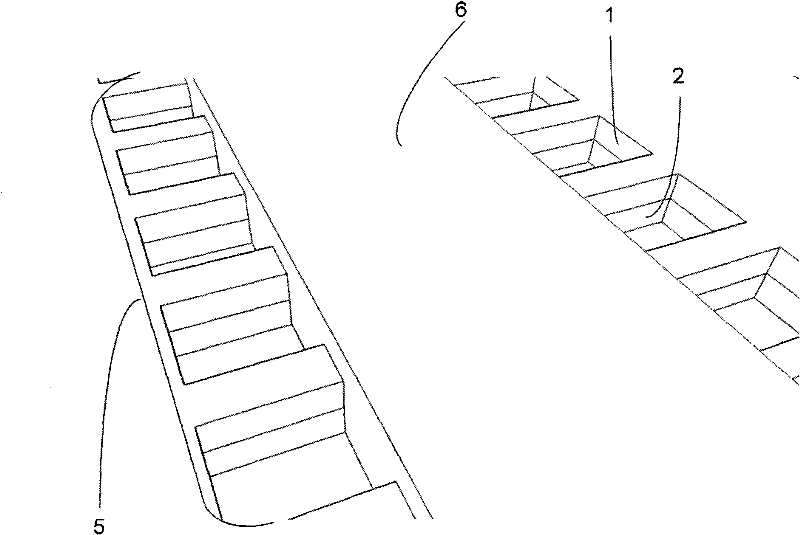
[0058] refer to Figure 1a , the Schottky gate heterojunction field effect transistor based on channel array structure is composed of heterojunction epitaxial material (including semiconductor 1 and semiconductor 2), source 3, drain 4, channel array 5 and gate 6 . Wherein, the semiconductor 1 and the semiconductor 2 constituting the heterojunction can be any semiconductor material that can form a two-dimensional electron gas 7 at the heterojunction. The two-dimensional electron gas 7 in the channel is adjusted and controlled through the gate 6, so as to control the device to be in the cut-off region, the linear region and the saturation region. The channel array 5 is formed by a plurality of channels 8 connected in parallel, and is located between the source 3 and the drain 4 and in the active region below the gate 6 . In this embodiment, the gate 6 is between the channel arrays 5, which can be Figure 1b and Figure 1c clearly seen in. And by figure 2 It can be seen tha...

Embodiment 2

[0060] refer to image 3 , the insulated gate heterojunction field effect transistor based on the channel array structure includes a semiconductor 1 , a semiconductor 2 , an insulating dielectric layer 9 and a gate 6 . A high-density two-dimensional electron gas exists at the heterojunction interface. An insulating dielectric layer covers the channel array 5 , and the uppermost layer is covered with gate metal to modulate the two-dimensional electron gas in the channel. Wherein, the insulating dielectric layer may be an oxide (such as silicon dioxide, aluminum oxide, hafnium oxide, etc.), or a non-oxide dielectric layer (such as silicon nitride, aluminum nitride, etc.). According to this embodiment, taking an AlGaN / GaN HEMT as an example, a layer of Al with a thickness of 10 nm is deposited between the gate 6 metal and AlGaN by ALD. 2 o 3 , can reduce the gate leakage current by four orders of magnitude, and effectively enhance the control ability of the gate to the channel...

Embodiment 3

[0062] refer to Figure 4 , the single channel heterojunction field effect transistor includes a semiconductor 1 , a semiconductor 2 , a source 3 , a drain 4 , a channel 8 and a gate 6 . A high-density two-dimensional electron gas 7 exists at the heterojunction interface. The device consists of a single channel 8, and the gate 6 covers both sides of the channel 8 to modulate the two-dimensional electron gas 7 at the heterointerface. The source 3 is grounded, and the drain 4 is applied with a forward voltage to make channel electrons flow from the source 3 to the drain 4 . According to this embodiment, taking the AlGaN / GaN heterojunction as an example, the width of the channel 8 is 500nm, the metal thickness of the gate 6 is 300nm, and the length of the gate 6 is 300nm. gs =1.5V when the saturation leakage current is 850mA / mm, the maximum peak transconductance is 195mS / mm, compared with the traditional AlGaN / GaN HEMT device at V gs The saturation leakage current at 1.5V is 5...


PUM

PropertyMeasurementUnit
Widthaaaaaaaaaa
Lengthaaaaaaaaaa
Thicknessaaaaaaaaaa

Abstract

The invention relates to a heterojunction field effect transistor based on a channel array structure. The heterojunction field effect transistor comprises a heterojunction which comprises a first semiconductor layer and a second semiconductor layer which are stacked from top to bottom; a two-dimensional electron gas is formed on the interface of the first semiconductor layer and the second semiconductor layer; a source electrode, a drain electrode and a grid electrode are arranged on the first semiconductor layer; the grid electrode is arranged between the source electrode and the drain electrode; and more than one channels are formed in the heterojunction under the grid electrode, and two ends of the channel respectively point to the source electrode and the drain electrode. In the invention, the structural design based on the channel array is adopted, and an annular gate structure is formed by covering a gate metal on the top part of the channel and the side walls on two sides, so that the capability of modulating the channel is strengthened. The heterojunction field effect transistor is suitable for all semiconductor electron devices working based on the two-dimensional electron gas on the heterojunction node interface, and various requirements of practical application can be met simultaneously.

Description

technical field [0001] The invention relates to a semiconductor electronic device, in particular to a heterojunction field effect transistor based on a channel array structure. Background technique [0002] A semiconductor heterojunction is composed of two or more different semiconductor materials. Due to the different physical and chemical parameters (such as electron affinity, energy band structure, dielectric constant, lattice constant, etc.) between different semiconductor materials, various physical and chemical properties will be mismatched at the contact interface, so that Heterojunctions have many new properties. The basic structure of a heterojunction field effect transistor consists of a heterojunction composed of a wide bandgap material and a narrow bandgap material. In this heterojunction, the N-type impurity-doped wide bandgap material acts as an electron supply layer to provide a large number of electrons to the undoped narrow bandgap material, or a large num...

Claims


Application Information

Patent Timeline
IPC IPC(8): H01L29/778H01L29/205H01L29/41
Inventor 蔡勇刘胜厚张宝顺
Owner SUZHOU INST OF NANO TECH & NANO BIONICS CHINESE ACEDEMY OF SCI
Why Eureka
Try Eureka