Partial silicon on insulator (PSOI) lateral super-junction power semiconductor device

A lateral super-junction power and semiconductor technology, applied in semiconductor devices, electrical components, circuits, etc., can solve the problems of reducing the withstand voltage of SOI lateral super-junction devices, charge imbalance, etc., to eliminate the substrate-assisted depletion effect, improve Charge balance, improve the effect of withstand voltage

Inactive Publication Date: 2011-09-28
ZHONGBEI UNIV
View PDF3 Cites 14 Cited by
  • Summary
  • Abstract
  • Description
  • Claims
  • Application Information

AI Technical Summary

Problems solved by technology

The charge imbalance between the N and P regions of the superjunc...

Method used


Image

  • Partial silicon on insulator (PSOI) lateral super-junction power semiconductor device
  • Partial silicon on insulator (PSOI) lateral super-junction power semiconductor device
  • Partial silicon on insulator (PSOI) lateral super-junction power semiconductor device

Examples


Embodiment Construction

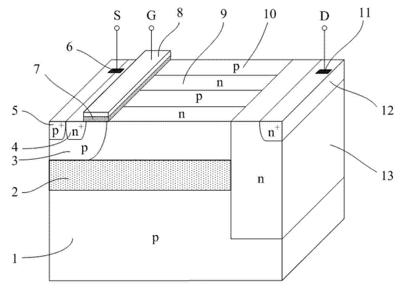
[0015] Attached below figure 1 The present invention will be described in detail.

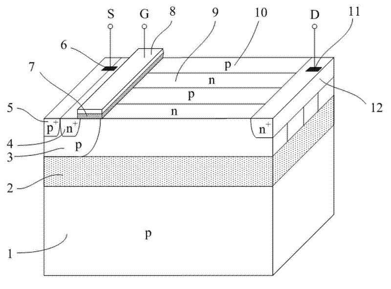
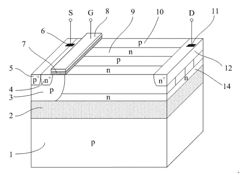
[0016] A PSOI lateral superjunction power semiconductor device according to the present invention comprises a p-type substrate 1, an insulating buried layer 2 is arranged on the upper end surface of the p-type substrate 1, and a p-type body region 3 is arranged on the upper end surface of the insulating buried layer 2 And the super junction structure, the super junction structure is composed of super junction n regions 9 and super junction p regions 10 distributed alternately in the lateral direction, the p type body region 3 is in contact with one side of the super junction structure, and the p type body region 3 is provided with n Type source region 4, p-type body contact region 5 and gate oxide layer 7, polysilicon gate 8 is arranged on the upper end of gate oxide layer 7, source electrode 6 is arranged on n-type source region 4 and p-type body contact region 5, super junction The other si...


PUM


Abstract

The invention discloses a PSOI lateral super-junction power semiconductor device. The PSOI lateral super-junction power semiconductor device comprises a semiconductor body, an insulation buried layer, a gate and an electrode, wherein the gate and the electrode are arranged on the semiconductor body, a super-junction structure is arranged above the insulation buried layer, consists of super-junction n regions and super-junction p regions in alternate distribution, and is connected with a p-type body region. An n-type compensation region arranged in a direction vertical to the super-junction structure is connected with the super-junction structure and the insulation buried layer, and extends into a substrate. By the invention, the substrate-assisted depletion effect existing in the lateral super-junction power device can be effectively inhibited so as to improve the voltage resistance of the device. Compared with the conventional charge-compensation lateral super-junction device, the PSOI lateral super-junction power semiconductor device can better keep the super-junction voltage resistance property without increasing the thickness of the top silicon because the n-type compensation region is vertical to the super-junction structure.

Description

technical field [0001] The invention belongs to the field of power semiconductor devices, in particular to SOI (Semiconductor On Insulator) lateral superjunction power semiconductor devices. Background technique [0002] Power semiconductor devices play an irreplaceable key role in the national economy and social life, and are widely used in consumer electronics, industrial control and defense equipment. Power semiconductor devices are also the key technology and basic technology for energy saving and emission reduction. Especially in my country, energy saving and consumption reduction is one of the basic national policies of the country. The development and promotion of semiconductor power devices is an important technical means for energy saving. [0003] Among power semiconductor devices, MOS type power devices (Power MOSFETs) can significantly reduce the switching time and increase the switching frequency of the device. However, in high-voltage applications, the on-resi...

Claims


Application Information

Patent Timeline
IPC IPC(8): H01L29/78H01L29/06
CPCH01L29/7824H01L29/0634H01L29/0882
Inventor 王文廉王玉王代华王巍赖富文张志杰
Owner ZHONGBEI UNIV
Why Eureka
Try Eureka