Integrated illuminating part and preparation method thereof
A technology of luminous parts and curing agents, which is applied in the direction of semiconductor devices, electrical components, circuits, etc., can solve the problems of reduced luminous efficiency, inconsistent color temperature, thickness sensitivity, etc., and achieve the effects of reduced reflection and scattering, stable quality, and easy operation
- Summary
- Abstract
- Description
- Claims
- Application Information
AI Technical Summary
Problems solved by technology
Method used
Image
Examples
Embodiment 1
[0025] Embodiment 1, as figure 1 As shown, an integrated light-emitting element includes a transparent substrate 3, a layer of phosphor layer 2 is arranged on the substrate 3, and the phosphor layer 2 is covered with a curing agent for curing the phosphor layer 2 on the substrate. Layer 1. The integrated light-emitting element in this embodiment is an integrated light-emitting panel. The substrate 3 is a glass plate, and the thickness of the substrate 3 is 0.5mm. The phosphor layer 2 is a YAG:Ce phosphor layer, and the thickness of the phosphor layer 2 is 40 μm. The curing agent is water glass. The substrate 3 is made of a hard material with a light-transmitting wavelength of 300nm-750nm, and can be a flat plate or other shapes, as long as it matches the shape of the LED.
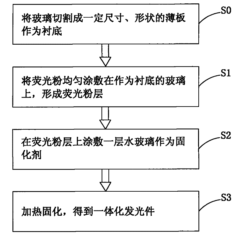
[0026] The preparation method of the integrated light-emitting element is to adopt the following steps:
[0027] (1) Coating a layer of fluorescent powder on the prepared substrate;
[0028] (2) coati...
Embodiment 2
[0036] Embodiment 2, an integrated light-emitting element, including a transparent substrate 3, a layer of phosphor layer 2 is arranged on the substrate 3, and the phosphor layer 2 is covered with a curing agent for curing the phosphor layer 2 on the substrate. agent layer 1. The substrate 3 in this embodiment is an epoxy resin board, and the thickness of the substrate 3 is 1 mm. The phosphor layer 2 is a mixture layer of yellow phosphor YAG:Ce and red phosphor CaS:Eu, and the thickness of the phosphor layer 2 is 30 μm. The curing agent is epoxy resin.
[0037] The preparation method of the integrated light-emitting element in this embodiment is the same as that in Embodiment 1, and will not be repeated here. The difference is that the coating method of the phosphor powder used is the sedimentation method, which is a prior art, and will not be described in detail here. Firstly, a phosphor layer with a thickness of 30 μm was prepared on the prepared epoxy resin plate by the ...
Embodiment 3
[0038] Embodiment 3, as figure 1 As shown, an integrated light-emitting element includes a transparent substrate 3, a layer of phosphor layer 2 is arranged on the substrate 3, and the phosphor layer 2 is covered with a curing agent layer for curing the phosphor layer 2 on the substrate. 1. The substrate 3 in this embodiment is a silica gel plate. The phosphor layer 2 is a yellow silicate phosphor layer (the yellow silicate phosphor is provided by Dalian Luming Lighting Technology Co., Ltd., the product model is LMS-560-B), and the thickness of the phosphor layer 2 is 20 μm. The curing agent is silica gel.
[0039] The preparation method of the integrated light-emitting element in this embodiment is the same as that in Embodiment 1, and will not be described again. The difference is that the phosphor powder used is sprayed, and the spraying method is a prior art, so it will not be described in detail here. . Firstly, a layer of yellow silicate phosphor powder with a thickne...
PUM
 Abstract
Description
Claims
Application Information


