Process for producing substrate provided with metal pattern and substrate provided with metal laminate
一种金属图案、制造方法的技术,应用在带金属图案的基板的制造及带金属层叠体的基板领域,能够解决金属膜能量吸收差、难以得到高输出激光、难加工等问题
- Summary
- Abstract
- Description
- Claims
- Application Information
AI Technical Summary
Problems solved by technology
Method used
Image

Examples
Embodiment approach 1
[0093] Figure 1 to Figure 7 It is a figure which shows an example of each process of the manufacturing method of the board|substrate with a metal pattern of Embodiment 1.
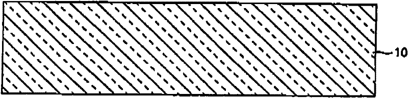
[0094] figure 1 It is a figure which shows an example of the process of preparing the board|substrate 10 in the manufacturing method of the board|substrate with a metal pattern of this embodiment. figure 1 The middle indicates a state in which the substrate 10 is placed and prepared. As the substrate 10 , substrates of various materials can be used, and it is preferable to use, for example, a glass substrate 10 . The glass substrate 10 is widely used as a display panel material of flat panel displays such as plasma display panels and liquid crystal panels. In the present embodiment, an example in which a glass substrate is used as the substrate 10 is described, but various substrates 10 can be used as long as the substrate 10 is resistant to heat generated during laser processing and laser irradiation a...
Embodiment approach 2
[0135] Figure 10 ~ Figure 14 It is a figure which shows an example of the manufacturing process of the manufacturing method of the board|substrate with a metal pattern of Embodiment 2.
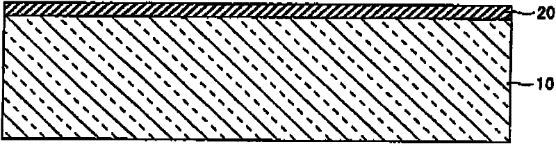
[0136] Figure 10 It is a figure which shows an example of the process of preparing the board|substrate 10 in the manufacturing method of the board|substrate with a metal pattern of Embodiment 2. Figure 10 The process shown is the same as that in Embodiment 1 figure 1 Since the steps described in are the same as those described in , the same reference numerals are attached and their descriptions are omitted.
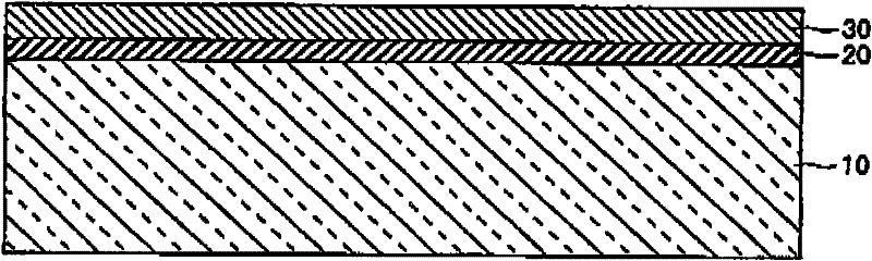
[0137] Figure 11 It is a figure which shows an example of the metal layer formation process of the manufacturing method of the board|substrate with a metal pattern of Embodiment 2. In the metal layer forming step, the metal layer 30 is formed on the substrate 10 . In Embodiment 1, the low-reflection layer 20 is formed on the substrate 10, but in the manufacturing method of the su...
example 1
[0151] Figure 15 (a) in (a) shows the result of Example 1. In Example 1, a copper (Cu) metal layer 30 was formed on a substrate 10 for a plasma display (PD), and laser processing was performed. The thickness of the copper metal layer 30 is As a result, it can be seen that if the metal layer 30 is copper alone, even if its surface is irradiated with a power of 74W and an energy density of 1.2J / cm 2 laser, even if its thickness is as thin as Also, the metal layer 30 could not be removed at all, so that a metal pattern could not be formed.
PUM
| Property | Measurement | Unit |
|---|---|---|
| wavelength | aaaaa | aaaaa |
| wavelength | aaaaa | aaaaa |
| coating thickness | aaaaa | aaaaa |
Abstract
Description
Claims
Application Information
 - R&D
- Intellectual Property
- Life Sciences
- Materials
- Tech Scout
- Unparalleled Data Quality
- Higher Quality Content
- 60% Fewer Hallucinations
Browse by: Latest US Patents, China's latest patents, Technical Efficacy Thesaurus, Application Domain, Technology Topic, Popular Technical Reports.
© 2025 PatSnap. All rights reserved.Legal|Privacy policy|Modern Slavery Act Transparency Statement|Sitemap|About US| Contact US: help@patsnap.com