Semiconductor radiation sensing device and manufacturing method thereof

A radiation-sensitive, semi-conductive technology, applied in semiconductor devices, final product manufacturing, sustainable manufacturing/processing, etc., can solve the problems of high lower limit of energy detection and low energy resolution, so as to improve energy resolution, reduce response time, The effect of reducing the lower limit of energy detection

Inactive Publication Date: 2011-10-12
PEKING UNIV
View PDF6 Cites 12 Cited by
  • Summary
  • Abstract
  • Description
  • Claims
  • Application Information

AI Technical Summary

Problems solved by technology

The energy resolution of the existing technology is

Method used


Image

  • Semiconductor radiation sensing device and manufacturing method thereof
  • Semiconductor radiation sensing device and manufacturing method thereof
  • Semiconductor radiation sensing device and manufacturing method thereof

Examples


Embodiment 1

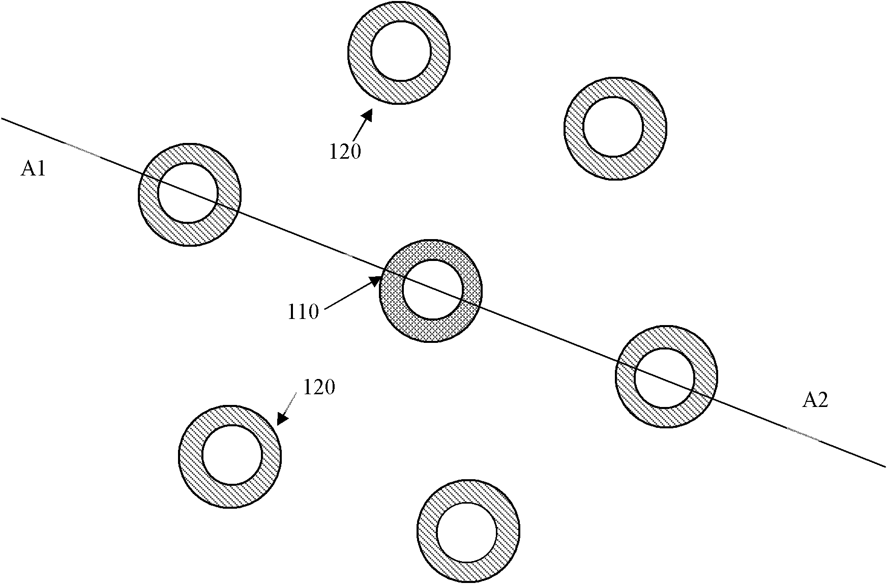
[0039] Figure 1~ Figure 5 As shown, the present invention provides a semiconductor radiation sensitive device, which contains at least one radiation sensitive unit. As shown in FIG. 1 , the radiation sensitive unit includes: a first substrate 100 , a first columnar electrode 110 , and a second columnar electrode 120 .

[0040] The first substrate 100 contains a first surface and a second surface;

[0041] The first columnar electrode 110 includes a first metal column 113 and N-type doped silicon 112 surrounding the first metal column;

[0042] The second columnar electrode 120 includes a second metal column 123 and a P-type doped silicon 122 surrounding the second metal column;

[0043] The first columnar electrode 110 and the second columnar electrode 120 are embedded inside the first substrate, vertically penetrating through the first surface and the second surface of the substrate;

[0044] The second columnar electrode 120 contains 6 metal columns arranged in a regular...

Embodiment 2

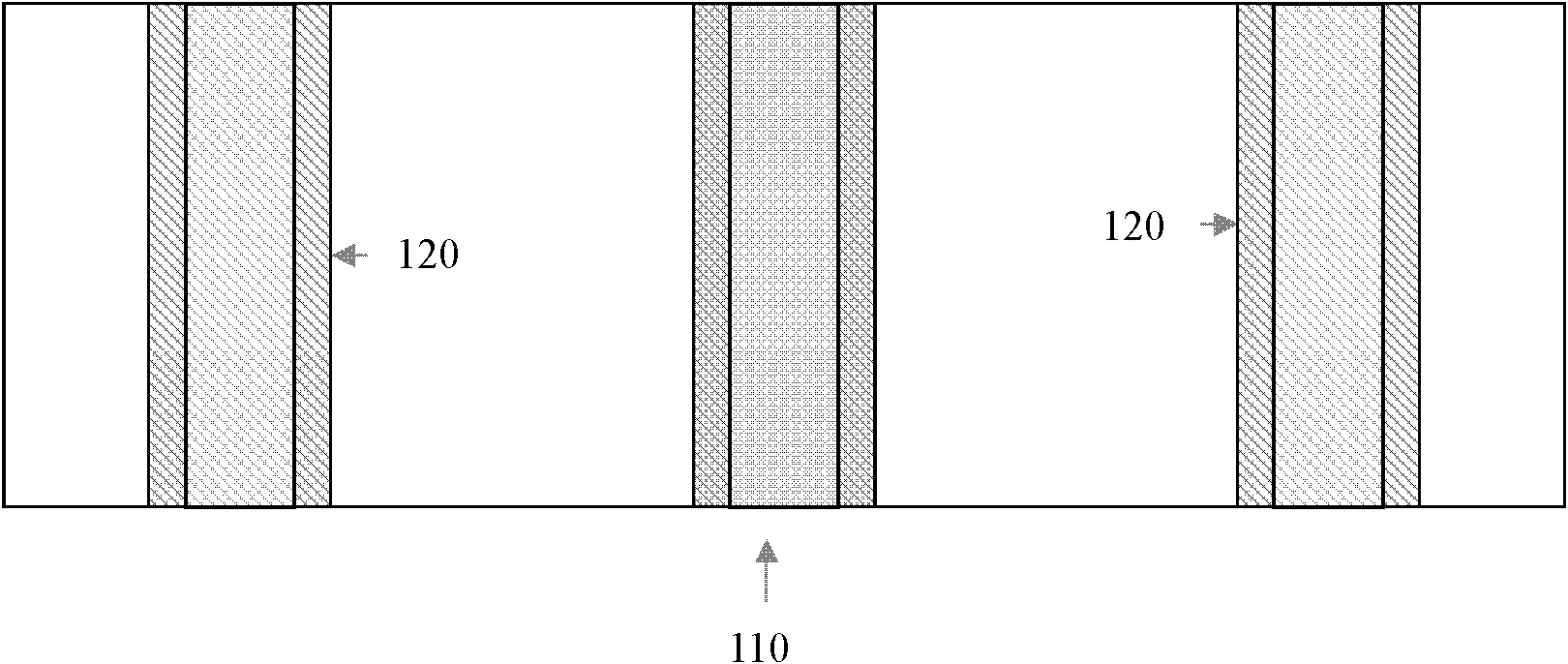
[0050] Figure 1~ Figure 5 As shown, the present invention provides a semiconductor radiation sensitive device, which includes at least one radiation sensitive unit and a signal processing circuit of the radiation sensitive unit, and the signal processing circuit is prior art. Radiation sensitive units such as Figure 5 As shown, it includes: a first substrate 100 , a first columnar electrode 110 , a second columnar electrode 120 , first pads 114 and 124 , and a second substrate 200 .

[0051] The structures of the first base body 100 , the first columnar electrode 110 , and the second columnar electrode 120 are the same as those in the first embodiment.

[0052] The first pad 114 is located at one end of the first columnar electrode 110 , and the first pad 124 is located at one end of the second columnar electrode 120 ;

[0053]The second substrate 200 is located on the first substrate 100;

[0054] The second substrate 200 contains a signal processing circuit and a second...

Embodiment 3

[0057] Figure 1~ Figure 5 As shown, the present invention provides a new manufacturing method designed for the above-mentioned semiconductor radiation sensitive device, comprising steps:

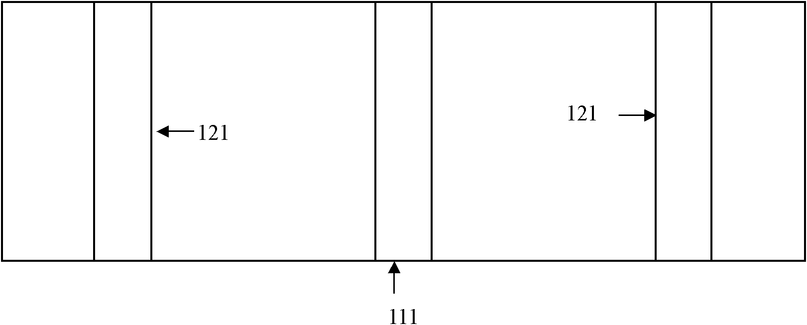
[0058] S1. A first wafer 100 is provided, and a first TSV through-silicon via 111 and a second TSV through-silicon via 121 are fabricated on the wafer, such as figure 2 shown. The fabrication of TSV through-silicon vias is as follows: coating photoresist, photolithography exposure, and development to make TSV through-silicon via mask; deep reactive ion (DRIE) etching through the silicon wafer to remove the photoresist. TSV through-silicon vias are also produced by double-sided photolithography and double-sided engraved holes; other methods, such as laser drilling, can also be used.

[0059] S2. Fabricate a first columnar electrode 110 and a second columnar electrode 120 in the TSVs 111 and 121 of the first wafer, respectively, as shown in FIG. 3 . The columnar electrodes are made in det...


PUM

PropertyMeasurementUnit
Resistivityaaaaaaaaaa

Abstract

The invention relates to the field of semiconductor sensors and discloses a semiconductor radiation sensing device and a manufacturing method thereof. The sensing device comprises at least one radiation sensing unit, wherein each radiation sensing unit comprises a first substrate, a first columnar electrode and a second columnar electrode; the first substrate comprises a first surface and a second surface; the first columnar electrode comprises first metal posts and N-type doped silicon surrounding the first metal posts; the second columnar electrode comprises more than two second metal postsand P-type doped silicon surrounding the second metal posts; the first columnar electrode and the second columnar electrode are embedded into the first substrate and pass through the first surface and the second surface of the substrate; the more than two metal posts are arranged in an equilateral polygon mode; and the first columnar electrode is arranged at the geometric center of the equilateral polygon. According to the invention, the thin dead layer thickness of the sensing device, the smaller equivalent capacitance and the shorter signal drifting process can be realized, thus improving the energy resolution, reducing the response time and decreasing the lower limit of energy detection.

Description

technical field [0001] The invention relates to the field of semiconductor sensors, in particular to a semiconductor radiation sensitive device and a manufacturing method thereof. Background technique [0002] Semiconductor radiation sensitive devices are widely used in nuclear experiments, space detection, biochemical defense, energy spectrum analysis and other fields; they mainly include: surface barrier sensitive devices, junction sensitive devices, silicon drift sensitive devices (Silicon Drift Detector, SDD) wait. Surface barrier sensitive device: Generally, an N-type single crystal silicon wafer is used and gold is deposited on it, so it is also often called a gold silicon surface barrier sensitive device. It uses the contact potential difference between gold and semiconductor to form a depletion layer without free carriers in the semiconductor, which is the sensitive area of ​​the sensitive device. Junction-sensitive devices, such as PIN-type sensitive devices: The ...

Claims


Application Information

Patent Timeline
IPC IPC(8): H01L31/10H01L31/0352H01L31/18
CPCY02P70/50
Inventor 马盛林
Owner PEKING UNIV
Why Eureka
Try Eureka