

Resistive random access memory with self-rectifying effect
A technology of resistive memory and resistive layer, applied in semiconductor devices, electric solid state devices, electrical components, etc., can solve the problems of increasing the complexity of device manufacturing and the influence of device miniaturization advantages, and achieves low cost and high compatibility. , to avoid the effect of crosstalk
- Summary
- Abstract
- Description
- Claims
- Application Information
AI Technical Summary
Problems solved by technology
Method used
Image

Examples
Embodiment 1
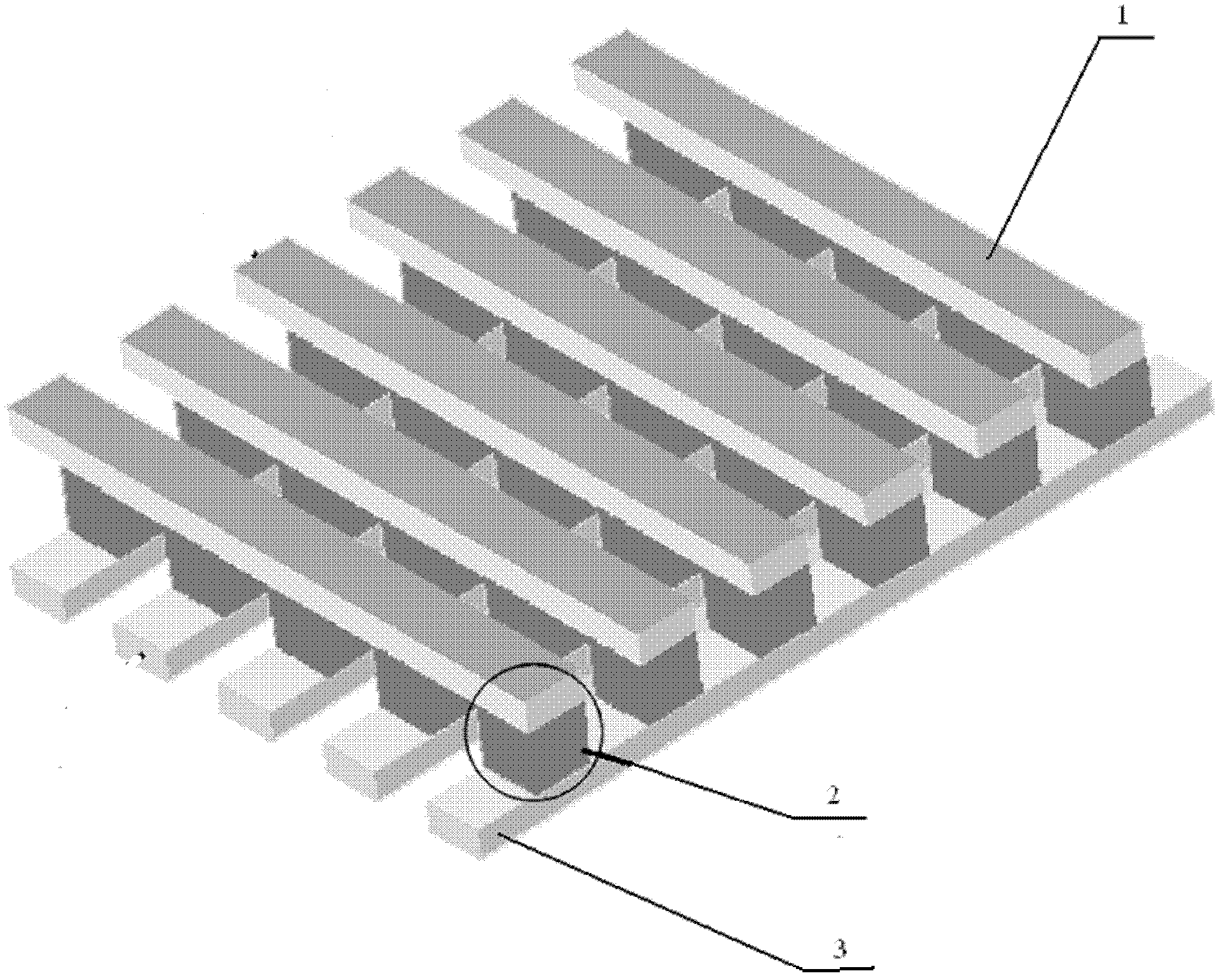
[0021] Embodiment 1. Fabrication of a resistive variable memory with a cross structure
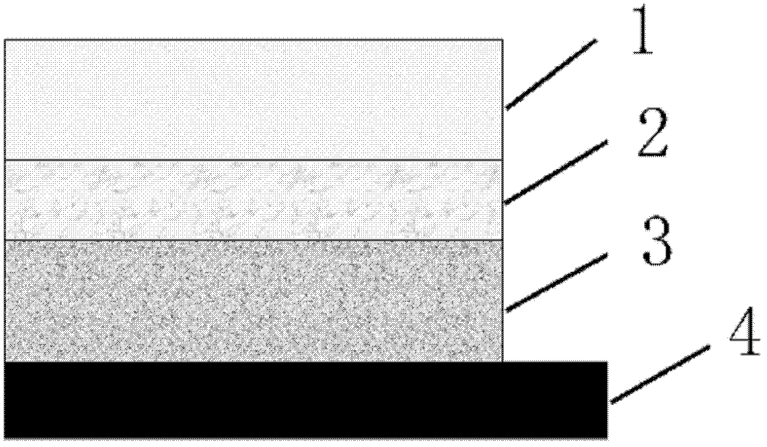
[0022] (1) A layer of insulating silicon oxide is obtained by high-temperature thermal oxidation on the silicon substrate, and a layer of p-type silicon heavily doped with B is deposited on the silicon oxide layer by pulsed electron beams, wherein the doping concentration of B is 10 20 cm -3 .
[0023] (2) Clean the p-type silicon with acetone, alcohol, and deionized water in sequence, and then dry it.
[0024] (3) Coating photoresist on the p-type silicon obtained above, and then exposing, the exposure intensity is 2.6mW / cm 2 ; Exposure time is 10 seconds; developing, developing for 1 minute, fixing for 30 seconds; then using reactive ion etching silicon substrate, the etching conditions are: RF power 50W, air pressure is 5Pa, SF6 gas flow rate is 40SCCM, The etching time is 100 seconds; finally, the photoresist is stripped off to obtain a strip-shaped p-type silicon bottom electrode w...
Embodiment 2
[0030] Embodiment 2, the making of the resistive variable memory of cross structure
[0031](1) A layer of insulating silicon oxide is obtained by high-temperature thermal oxidation on the silicon substrate, and a layer of p-type silicon material heavily doped with Al is deposited on the silicon oxide layer by pulsed electron beam, wherein the doping concentration of Al is 10 20 cm -3 .
[0032] (2) Clean the p-type silicon with acetone, alcohol, and deionized water in sequence, and then dry it.
[0033] (3) Coating photoresist on the p-type silicon obtained above, and then exposing, the exposure intensity is 2.6mW / cm 2 ; Exposure time is 10 seconds; developing, developing for 1 minute, fixing for 30 seconds; then using reactive ion etching silicon substrate, the etching conditions are: RF power 50W, air pressure is 5Pa, SF6 gas flow rate is 40SCCM, The etching time is 100 seconds; finally, the photoresist is stripped off to obtain a strip-shaped p-type silicon bottom elect...
Embodiment 3
[0039] Embodiment 3, Fabrication of a resistive variable memory with a cross structure
[0040] (1) A layer of insulating silicon oxide is obtained by high-temperature thermal oxidation on the silicon substrate, and a layer of p-type silicon material heavily doped with Ga is deposited on the silicon oxide layer by pulsed electron beam, wherein the doping concentration of Ga is 10 20 cm -3 .
[0041] (2) Clean the p-type silicon with acetone, alcohol, and deionized water in sequence, and then dry it.
[0042] (3) Coating photoresist on the p-type silicon obtained above, and then exposing, the exposure intensity is 2.6mW / cm 2 ; Exposure time is 10 seconds; developing, developing for 1 minute, fixing for 30 seconds; then using reactive ion etching silicon substrate, the etching conditions are: RF power 50W, air pressure is 5Pa, SF6 gas flow rate is 40SCCM, The etching time is 100 seconds; finally, the photoresist is stripped off to obtain a strip-shaped p-type silicon bottom e...
PUM
| Property | Measurement | Unit |
|---|---|---|
| Thickness | aaaaa | aaaaa |
| Resistivity | aaaaa | aaaaa |
| Resistivity | aaaaa | aaaaa |
Abstract
Description
Claims
Application Information