Production technology of semiconductor grade silicon single crystal

A production process, monocrystalline silicon technology, applied in the field of semiconductor-grade monocrystalline silicon production technology, can solve the problems of difficult control of product quality, easy occurrence of eddy defects, poor uniformity of cross-sectional resistivity, etc., to achieve convenient implementation and easy to master, improve The uniformity of cross-sectional resistivity and the effect of accelerating production efficiency

Inactive Publication Date: 2011-10-19
XIAN HUAJING ELECTRONICS TECH
View PDF7 Cites 14 Cited by
  • Summary
  • Abstract
  • Description
  • Claims
  • Application Information

AI Technical Summary

Problems solved by technology

However, the semiconductor-grade monocrystalline silicon currently on the market has various defects and deficiencies such as poor uniformity of cross-sectional resistivity, easy occurrence of swirl defects, and difficult control of product quality.

Method used


Image

  • Production technology of semiconductor grade silicon single crystal
  • Production technology of semiconductor grade silicon single crystal

Examples


Embodiment Construction

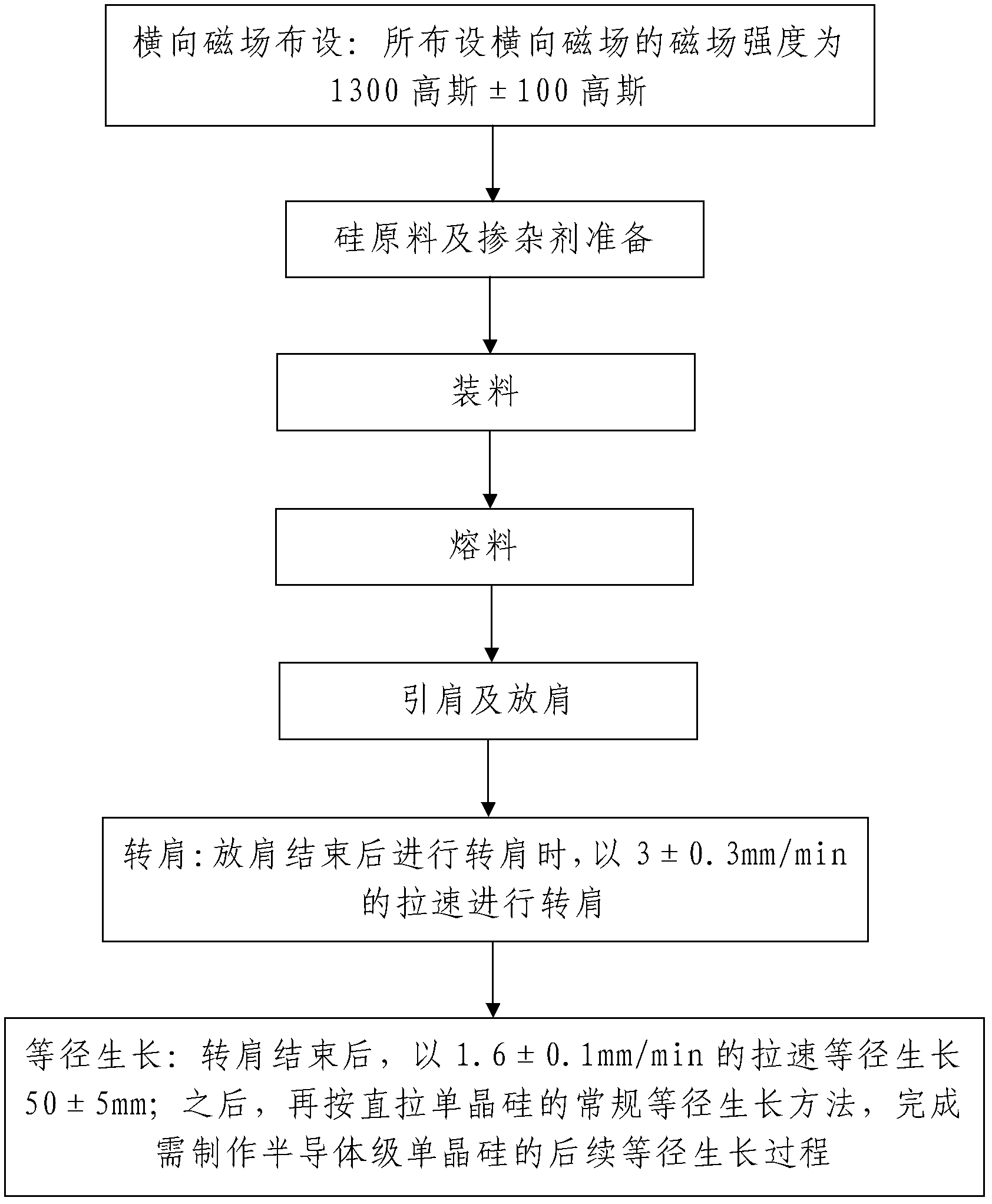
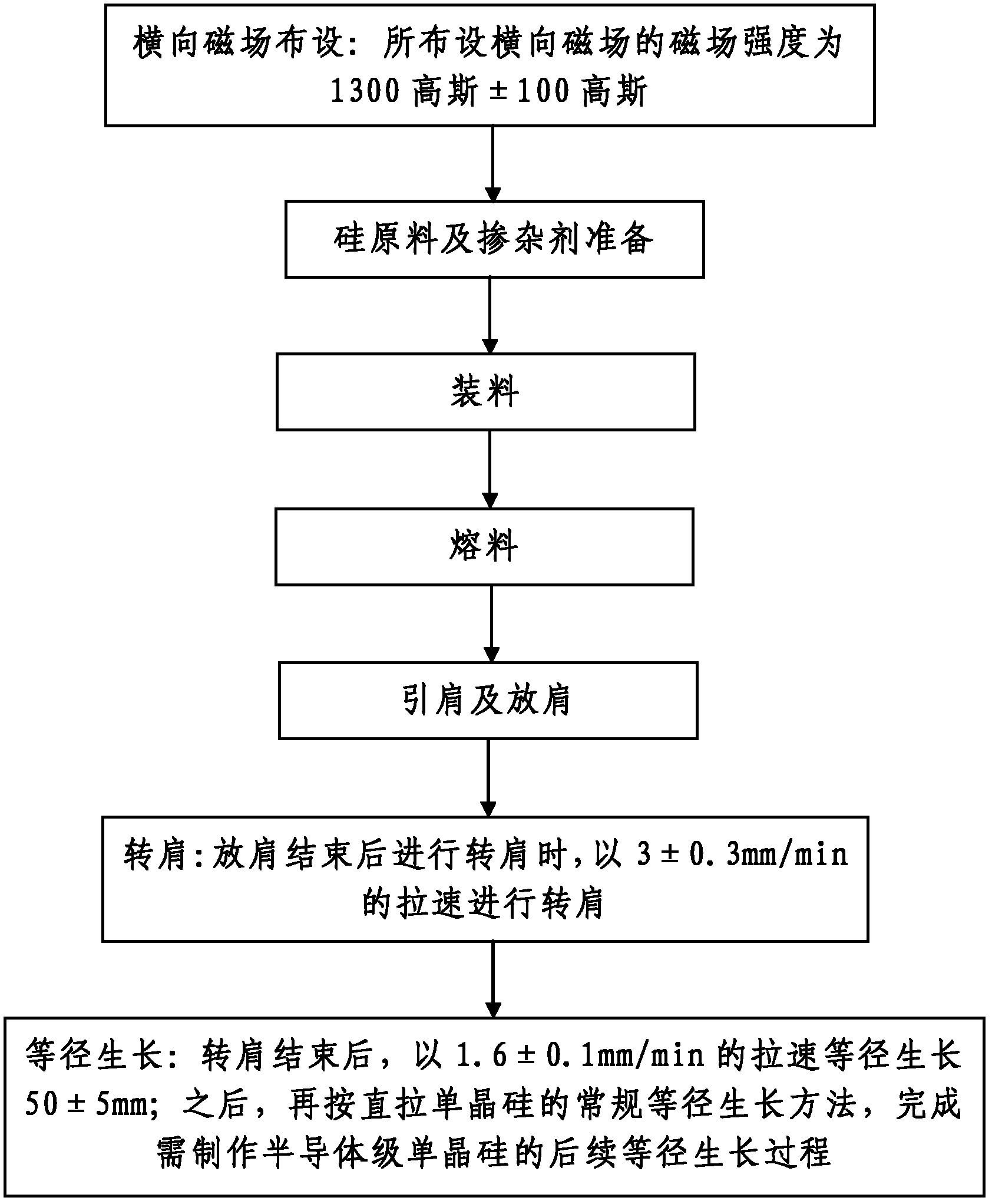
[0037] Such as figure 1 A semiconductor-grade monocrystalline silicon production process shown includes the following steps:

[0038] Step 1. Transverse magnetic field arrangement: a transverse magnetic field is arranged outside the middle part of the main furnace chamber 1 of the single crystal furnace that needs to produce semiconductor-grade single crystal silicon, and the magnetic field strength of the transverse magnetic field is 1300 Gauss ± 100 Gauss. Among them, 1 Gauss=1 Oersted. It can also be said that the magnetic field strength of the transverse magnetic field is 1300 Oersted±100 Oersteds.

[0039] When the transverse magnetic field is actually laid out, the magnetic field strength of the transverse magnetic field is 1300 Gauss±20 Gauss. In this embodiment, the magnetic field strength of the transverse magnetic field is 1300 Gauss. During actual use, the magnetic field strength of the transverse magnetic field can be adjusted accordingly according to actual need...


PUM

PropertyMeasurementUnit
magnetic flux densityaaaaaaaaaa

Abstract

The invention discloses a production technology of semiconductor grade silicon single crystal, comprising the following steps: 1, arranging a transverse magnetic field: the magnetic field intensity of the transverse magnetic field is 1300 + / - 100 gausses; 2, preparing silicon material and doping agent; 3, charging; 4, melting material; 5, introducing shoulder and expanding shoulder; 6, rotating shoulder: after the step of expanding shoulder, the step of rotating shoulder is carried out with a casting speed of 3 + / - 0.3 mm / min; and 7, growing at the same diameter: after the step of rotating shoulder, the material grows up to 50 + / - 5 mm with a casting speed of 1.6 + / - 0.1 mm / min; then, a conventional method of growing at the same diameter for direct pulling silicon single crystal is used to complete the subsequent process of growing at the same diameter of the semiconductor grade silicon single crystal. The method has the advantages of reasonable design, simple steps, easiness in realization, easiness in mastering and good using effect, and is capable of effectively guaranteeing the quality of the produced semiconductor grade silicon single crystal. The produced semiconductor grade silicon single crystal has high uniformity of cross-section electric resistivity and no micro-defects such as swirl.

Description

technical field [0001] The invention belongs to the technical field of monocrystalline silicon production, and in particular relates to a semiconductor-grade monocrystalline silicon production process. Background technique [0002] Monocrystalline silicon, also known as monocrystalline silicon, is a semiconductor material. In recent years, with the rapid development of the photovoltaic industry, monocrystalline silicon has been used to make solar cells, showing a situation in which demand exceeds supply. With the development of high technology, it is the common wish of every material manufacturer and device manufacturer to produce nearly perfect high-quality single crystal silicon. This kind of single crystal silicon has good cross-sectional resistivity uniformity, high life, and low carbon content. , Micro-defect density is small, and the oxygen content can be controlled. [0003] At present, the methods for producing single crystal silicon include Czochralski method, zon...

Claims


Application Information

Patent Timeline
Patent Type & Authority Applications(China)
IPC IPC(8): C30B15/20C30B29/06
Inventor 周建华
Owner XIAN HUAJING ELECTRONICS TECH
Why Eureka
Try Eureka