

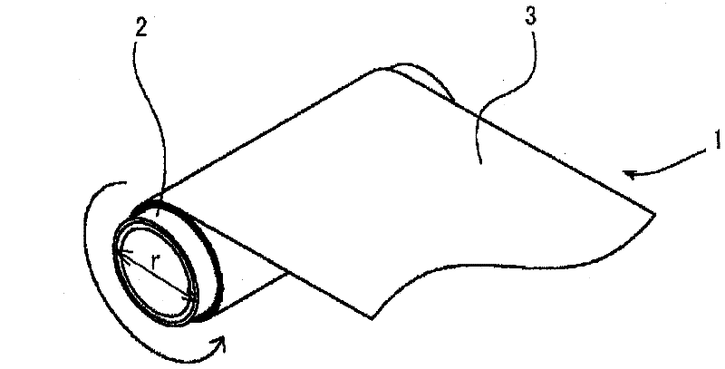
Film roll for producing semiconductor device
A technology of semiconductor and film roll, applied in semiconductor/solid-state device manufacturing, semiconductor device, semiconductor/solid-state device parts and other directions, can solve the problem of inability to adhere semiconductor chips or adherends, semiconductor chips fall off, and inability to exert adhesive force and other problems, to achieve the effects of excellent adhesion, prevention of curling marks, and good adhesiveness
- Summary
- Abstract
- Description
- Claims
- Application Information
AI Technical Summary
Problems solved by technology
Method used
Image

Examples
Embodiment 1
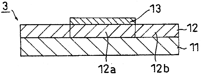
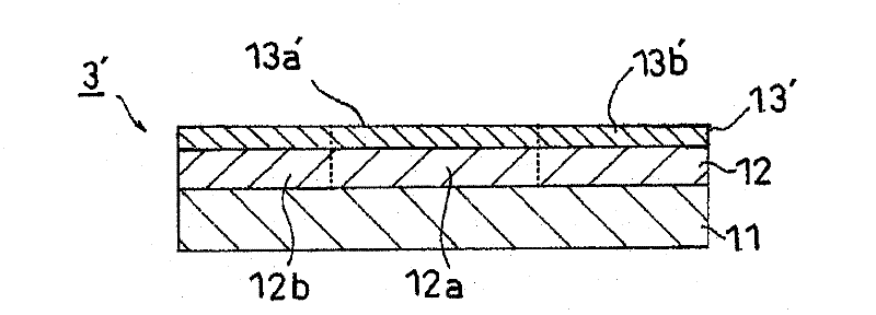
[0099] 3 parts by weight of a polyfunctional isocyanate crosslinking agent, 23 Parts by weight of epoxy resin (manufactured by Japan Epoxy Resin Co., Ltd., Epicoat 1004), 6 parts by weight of phenolic resin (manufactured by Mitsui Chemicals Co., Ltd., Mirex XLC-LL) and 60 parts by weight of spherical silica (manufactured by Admatex Co., Ltd., S0 -25R) was dissolved in methyl ethyl ketone to prepare an adhesive composition solution with a concentration of 20% by weight.
[0100] This adhesive composition solution was coated on a release-treated film (core material) made of a polysiloxane release-treated polyethylene terephthalate film (thickness 50 μm) as a release liner, Dry at 120°C for 3 minutes. Thus, an adhesive bond layer with a thickness of 25 μm was formed on the release-treated film.
[0101] Then, the solution of the acrylic adhesive composition was coated on a substrate made of a polyolefin film with a thickness of 100 μm and dried to form an adhesive layer with a ...
Embodiment 2
[0106] In Example 2, the film roll of this Example was produced in the same manner as in Example 1, except that a core with a diameter of 6 inches (15.24 cm) was used instead of a core with a diameter of 3 inches (7.62 cm).
Embodiment 3
[0108] In this Example 3, 50 sheets of dicing / die-bonding film were wound onto a core with a diameter of 3 inches (7.62 cm), and the diameter of the rolled film roll was 11.3 cm. Example 1 is operated in the same manner to make the film roll of this embodiment.
PUM
| Property | Measurement | Unit |
|---|---|---|
| diameter | aaaaa | aaaaa |
| thickness | aaaaa | aaaaa |
| diameter | aaaaa | aaaaa |
Abstract
Description
Claims
Application Information