
System for detecting capacitance C in micro area of electronic component

A technology of electronic components and micro-area, applied in the direction of measuring resistance/reactance/impedance, instruments, measuring devices, etc., can solve the problems of unavailability, large error, poor 2DEG concentration accuracy, etc., to eliminate stray capacitance, improve The effect of accuracy

Inactive Publication Date: 2011-11-02
UNIV OF ELECTRONICS SCI & TECH OF CHINA
View PDF5 Cites 2 Cited by
  • Summary
  • Abstract
  • Description
  • Claims
  • Application Information

AI Technical Summary

Problems solved by technology

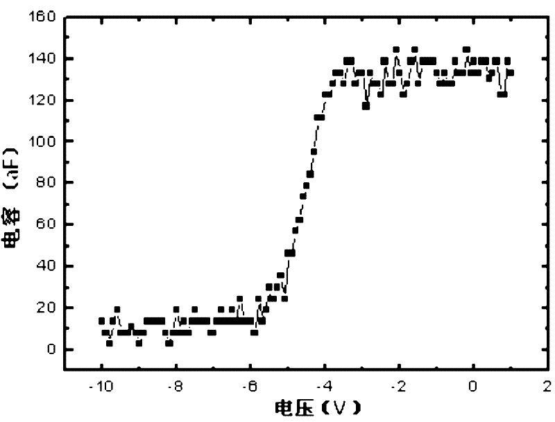
According to the above formula, in order to detect the 2DEG electron gas concentration n, it is necessary to measure the capacitance value C of the micro-area, because the capacitance value C of the micro-area cannot be obtained by using the scanning probe microscope to detect the capacitance of the micro-area of ​​electronic components. The value of C can be ignored (that is, the numerator of the formula is set to 1), and the obtained concentration value of 2DEG can only be an approximate value
That is, only qualitative analysis can be carried out on the concentration of 2DEG, but not quantitative analysis, thus affecting the accurate evaluation of the electrical and physical properties of the device; in addition, due to the influence of stray capacitance in the test, the obtained dC / dV The error of the value (change rate) is also large, so the accuracy of the qualitative analysis of the 2DEG concentration is also poor

Method used


Image

  • System for detecting capacitance C in micro area of electronic component
  • System for detecting capacitance C in micro area of electronic component
  • System for detecting capacitance C in micro area of electronic component

Examples


Embodiment Construction

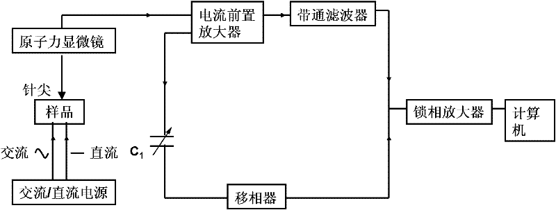
[0013] In this embodiment: the model of the atomic force microscope is (SPA-300HV), and the current preamplifier adopts an "integrator-differentiator" structure, and its input stage is composed of an operational amplifier OPA627B and a feedback capacitor (OPA627B has a low-noise, high-bandwidth Features, the voltage noise density at 10kHz is less than 4.5nV / √Hz, the bias current is only 1pA, the current noise density at 100Hz is less than 2.5fA / √Hz), the bandpass filter adopts the 5113 bandpass filter produced by Signal Recovery , the lock-in amplifier model is SR830, the variable capacitor C 1 The present embodiment adopts the variable capacitor whose adjustment range is 0.1-50pF, the phase shifter adopts a 180° phase shifter, the computer (processor) adopts a conventional general-purpose computer, and the AC / DC power supply adopts 0.1-100kHz and a voltage of 0.1 -5V AC and -50-50V AC / DC power supply with variable DC voltage.

[0014] In this embodiment, the detection of an ...


PUM


Abstract

The invention relates to a system for detecting the capacitance C in a micro area of an electronic component and belongs to an instrument for electronic component testing. The system comprises an atomic force microscope, an alternating current / direct current power supply for electric signal loading, a current preamplifier, a band-pass filter, a phase locking amplifier, a data acquisition card, a computer connected with the data acquisition card, and a phase shift circuit with an adjustable capacitor and a phaser. By arranging the current preamplifier and the band-pass filter between the atomic force microscope and the phase locking amplifier, and connecting the phase shift circuit with the adjustable capacitor and the phaser in parallel between the inverted input end of the current preamplifier and the input end of the phase locking amplifier, the system provided by the invention ensures that the capacitance C can be measured and the influence of stray capacitance can be eliminated, thus, the capacitance C in the micro area of the electronic component can be accurately measured, and the detection accuracy of the dC / dV value (rate of change) of the electronic component can be improved, thereby providing an accurate basis for the physical and electric performance analysis of the electronic component.

Description

technical field [0001] The invention belongs to the field of testing instruments and testing technologies for electronic components, in particular to a detection system for detecting the capacitance value of a tiny area (point area) of an electronic component based on an atomic force microscope (AFM). The detection system can be used to quantitatively detect the capacitance value of a small area (point area) specified by electronic components such as thin films and the change value of the point capacitance, and provide a basis for further analysis of the physical and electrical properties of electronic components. Background technique [0002] For the characterization of the physical and electrical properties of electronic components, a very important method is to use the capacitance-voltage (C-V) detection method. The data obtained by this detection method can be used to judge the carrier type, doping concentration, depletion The layer width and the analysis of the electric...

Claims


Application Information

Patent Timeline
Patent Type & Authority Applications(China)
IPC IPC(8): G01R27/26
Inventor 曾慧中韩若冰王志红林媛黄文
Owner UNIV OF ELECTRONICS SCI & TECH OF CHINA
Learn More