P type metal oxide semiconductor transistor for plasma display panel (PDP) driving chip

A technology for driving chips and semiconductor tubes, which is applied in semiconductor devices, electrical components, circuits, etc., can solve the problems of easy breakdown of N-type epitaxial layers, and achieve the effects of saving chip area, fully compatible processes, and simple structure

Inactive Publication Date: 2011-11-02
SICHUAN CHANGHONG ELECTRIC CO LTD
View PDF5 Cites 0 Cited by
  • Summary
  • Abstract
  • Description
  • Claims
  • Application Information

AI Technical Summary

Problems solved by technology

[0003] The purpose of the present invention is to overcome the easy breakdown of the N-type epitaxial layer between the source end power supply of the high-end P-type metal-oxide-semiconductor tube in the level shift circuit of the current PDP driver chip and the isolation groove The disadvantages of providing a PDP driver chip PMOS

Method used


Image

  • P type metal oxide semiconductor transistor for plasma display panel (PDP) driving chip
  • P type metal oxide semiconductor transistor for plasma display panel (PDP) driving chip
  • P type metal oxide semiconductor transistor for plasma display panel (PDP) driving chip

Examples


Embodiment

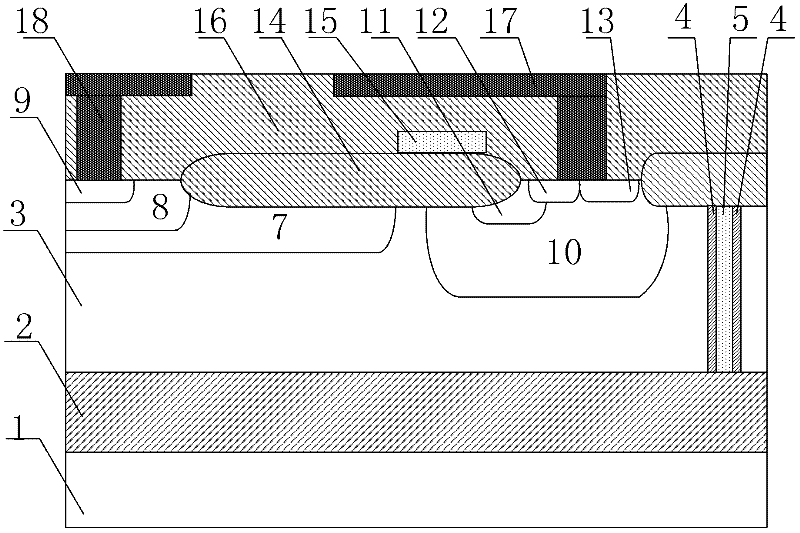
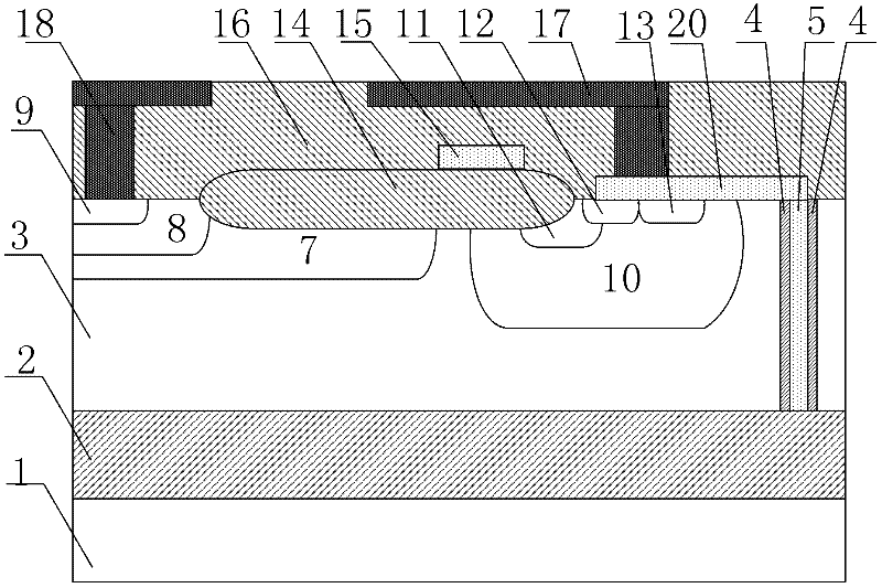
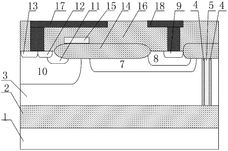
[0016] The cross-sectional view of the P-type metal oxide semiconductor tube of the PDP driver chip in this example is as follows image 3 .

[0017] The upper surface of the P-type drain end ohmic contact region 9 of the P-type metal oxide semiconductor transistor of the PDP driver chip is connected to the drain end metal 18, and the rest is arranged in the P-type buffer area 8, and the P-type buffer area 8 is arranged in the In the high-voltage P-type well 7, the isolation trench is arranged between the field oxide layer 14 and the buried oxide layer 2 at the drain position in the N-type epitaxial layer 3, and the horizontal distance between the isolation trench and the high-voltage P-type well 7 is not 0, and every Each isolation trench is composed of a polysilicon layer 5 and two sidewall oxide layers 4, wherein a polysilicon layer 5 is arranged between the field oxide layer 14 and the buried oxide layer 2 at the drain position in the N-type epitaxial layer 3, and the poly...


PUM


Abstract

The invention relates to a semiconductor technology and provides a P type metal oxide semiconductor transistor for a plasma display panel (PDP) driving chip, and the P type metal oxide semiconductor transistor can be used for solving the problem that an N type epitaxial layer of a P type metal oxide semiconductor transistor between the source end power source of the high-end P type metal oxide semiconductor transistor and an isolation groove in a level shift circuit is easy to break down. The technical scheme is as follows: in the P type metal oxide semiconductor transistor for the PDP driving chip, the upper surface of the ohmic contact area of a P type drain terminal is connected with a metal at the drain terminal, the rest parts are arranged in a P type buffer area; the P type buffer area is arranged in a high-voltage P type trap; the isolation groove is arranged between an oxide layer and a buried oxide layer in the N type epitaxial layer, wherein the drain electrode in the oxide layer is epitaxial; and the horizontal distance between the isolation groove and the high-voltage P type trap is not equal to zero outside the ohmic contact area of the P type drain terminal. The semiconductor transistor has the beneficial effects that the N type epitaxial layer is not easy to break down and is suitable for the P type metal oxide semiconductor transistor for the PDP driving chip.

Description

technical field [0001] The invention relates to a semiconductor (Silicon On Insulator) technology, in particular to a P-type metal oxide semiconductor tube used in a PDP (Plasma Display Panel) driver chip. Background technique [0002] As the mainstream flat-panel display in the market, PDP has the characteristics of large viewing angle, fast response, small thickness, large screen and full digital work. It is an ideal display device for high-definition digital TV, large wall-mounted TV and multimedia terminal. The PDP driver chip involves When it comes to high-voltage power integrated circuits, which have high technical content, the design and isolation of high-voltage devices in the chip are the key. Compared with bulk silicon technology, SOI (Silicon On Insulator) technology has the advantages of high speed, low power consumption, high integration and easy isolation, etc., and weakens the latch-up effect and has strong radiation resistance, making the integrated circuit ...

Claims


Application Information

Patent Timeline
IPC IPC(8): H01L29/78H01L29/06H01L29/08
Inventor 廖红
Owner SICHUAN CHANGHONG ELECTRIC CO LTD
Why Eureka
Try Eureka