Formation method of LED

A LED structure and semiconductor technology, which is applied in the direction of electrical components, circuits, semiconductor devices, etc., can solve problems such as film cracks, limit the thickness of epitaxial films, and poor film quality, so as to reduce manufacturing costs, facilitate heat dissipation, reduce The effect of thickness

Inactive Publication Date: 2011-11-02
淄博瑞创能科电子技术有限公司
View PDF9 Cites 6 Cited by
  • Summary
  • Abstract
  • Description
  • Claims
  • Application Information

AI Technical Summary

Problems solved by technology

[0003] However, there is a large lattice mismatch and thermal stress mismatch between Si and these III-V materials. The lattice mismatch causes dislocations, and the thermal str

Method used


Image

  • Formation method of LED
  • Formation method of LED
  • Formation method of LED

Examples


Embodiment Construction

[0026] Embodiments of the present invention are described in detail below, examples of which are shown in the drawings, wherein the same or similar reference numerals designate the same or similar elements or elements having the same or similar functions throughout. The embodiments described below by referring to the figures are exemplary only for explaining the present invention and should not be construed as limiting the present invention.

[0027] The following disclosure provides many different embodiments or examples for implementing different structures of the present invention. To simplify the disclosure of the present invention, components and arrangements of specific examples are described below. Of course, they are only examples and are not intended to limit the invention. Furthermore, the present invention may repeat reference numerals and / or letters in different instances. This repetition is for the purpose of simplicity and clarity and does not in itself indicat...


PUM


Abstract

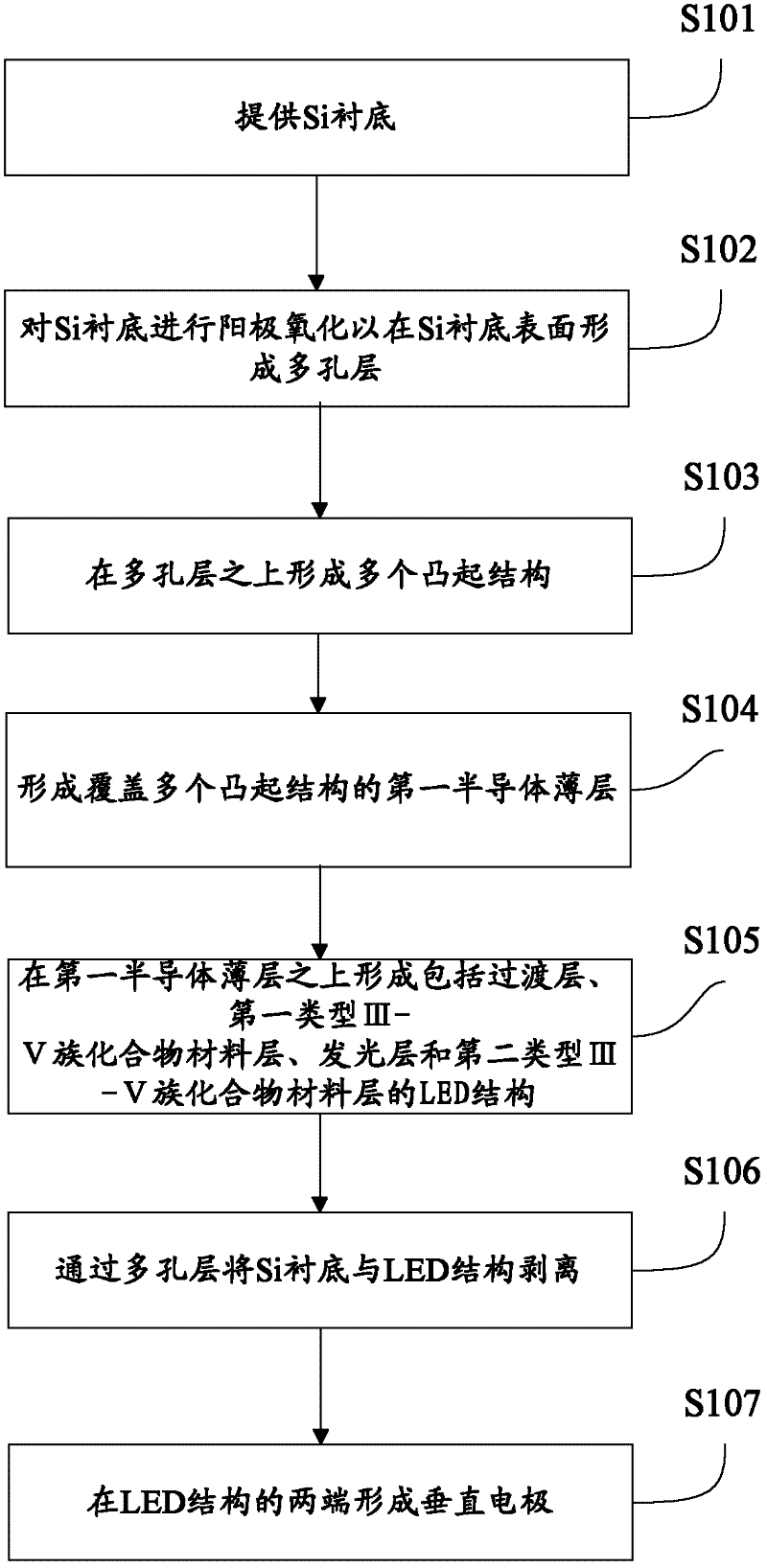
The invention provides a formation method of a light emitting diode (LED). The method comprises the following steps that: a Si substrate is provided; a plurality of projection structures are formed on the Si substrate, wherein there is a certain gap between each two projection structures; a first semiconductor thin layer is formed to cover the plurality of projection structures and is connected with tops of the plurality of projection structures; and an LED structure, which contains a first-type group III-V compound material layer, a luminescent layer, a second type group III-V compound material layer, is formed on the first semiconductor thin layer. The plurality of projection structures enable a heat mismatch stress between an Si wafer and a semiconductor material layer of nitride-system compound to be released effectively, so that a large-sized epitaxial wafer can be formed favorably.

Description

technical field [0001] The invention relates to the technical field of semiconductor design and manufacture, in particular to a method for forming an LED (light emitting diode). Background technique [0002] With the continuous progress of green energy, light emitting diodes (light emitting diodes, LEDs) are widely used in display screens, backlights, special lighting and other fields due to their long life, high luminous efficiency, small size, durability, and rich colors. The core of the LED is the LED epitaxial wafer, and its main structure includes: a substrate, a buffer layer, an N-type semiconductor layer, an active region light-emitting layer, an electron blocking layer, and a P-type semiconductor layer. As the core of the LED epitaxial wafer, the light-emitting layer in the active area is between the N-type semiconductor layer and the P-type semiconductor layer, so that the interface between the P-type semiconductor layer and the N-type semiconductor layer forms a PN...

Claims


Application Information

Patent Timeline
IPC IPC(8): H01L33/00H01L21/78
Inventor 李园赵东晶
Owner 淄博瑞创能科电子技术有限公司
Why Eureka
Try Eureka