GaAs/Si epitaxial material preparation method

An epitaxial material and seed layer technology, which is used in the growth of polycrystalline materials, chemical instruments and methods, semiconductor/solid-state device manufacturing, etc. dislocation effect

Inactive Publication Date: 2017-02-22
DONGGUAN LIANZHOU INTPROP OPERATION MANAGEMENT CO LTD
View PDF10 Cites 5 Cited by
  • Summary
  • Abstract
  • Description
  • Claims
  • Application Information

AI Technical Summary

Problems solved by technology

In the prior art, there are reports of using molecular beam epitaxy (Molecular BeamEpitaxy, MBE) to grow In(Ga)As quantum dot dislocation barriers to reduce the dislocation density of GaAs / Si epitaxial materials, but the growth rate is slow and multilayer In(Ga)As quantum dot dislocation barrier layer will accumulate strong compressive strain energy in GaAs / Si epitaxial materials, so that the prepared materials have greater stress
Chinese Invention Patent Publication No. 201410514645.7 introduces a MOCVD preparation method of GaAs / Si epitaxial materials. The propagation direction of dislocations in the epitaxial materials is changed through a multi-layer quantum dot dislocation barrier layer to reduce dislocations. The process is: using MOCVD Method A GaAs low-temperature nucleation layer, medium-temperature buffer layer, first high-temperature buffer layer, second high-temperature buffer layer, temperature-variable buffer layer, multi-layer quantum dot dislocation barrier layer and strain insertion layer were sequentially grown on a clean single crystal silicon substrate , and finally grow the GaAs epitaxial layer, the process is complicated, and although the strain energy of the multilayer quantum dot dislocation barrier layer can be balanced by the tensile stress of the strained superlattice, thereby reducing or eliminating the total strain energy of the material, it is still There are stress worries
Therefore, the method of reducing dislocations in the epitaxial material by the stress field is prone to cracks in the subsequent device fabrication and reduces the quality of the device.

Method used


Image

  • GaAs/Si epitaxial material preparation method
  • GaAs/Si epitaxial material preparation method

Examples


Embodiment 1

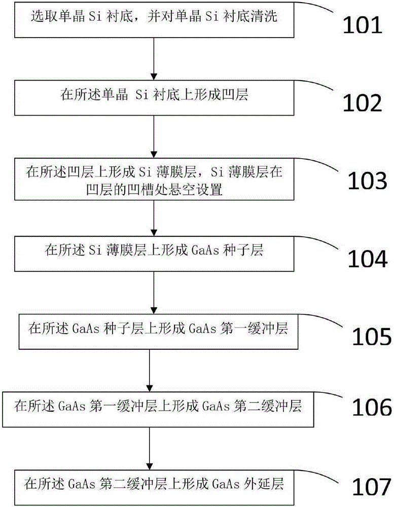
[0035] Step 101: Select a single crystal Si substrate 1 and clean the single crystal Si substrate 1 .

[0036] The crystal plane of the single crystal Si substrate 1 is the (100) crystal plane, which is an intrinsic type n-type silicon wafer with a thickness of 400 μm, and the growth of silicon is biased to the (011) crystal plane by 6° to form diatomic steps and suppress Reverse domain formation.

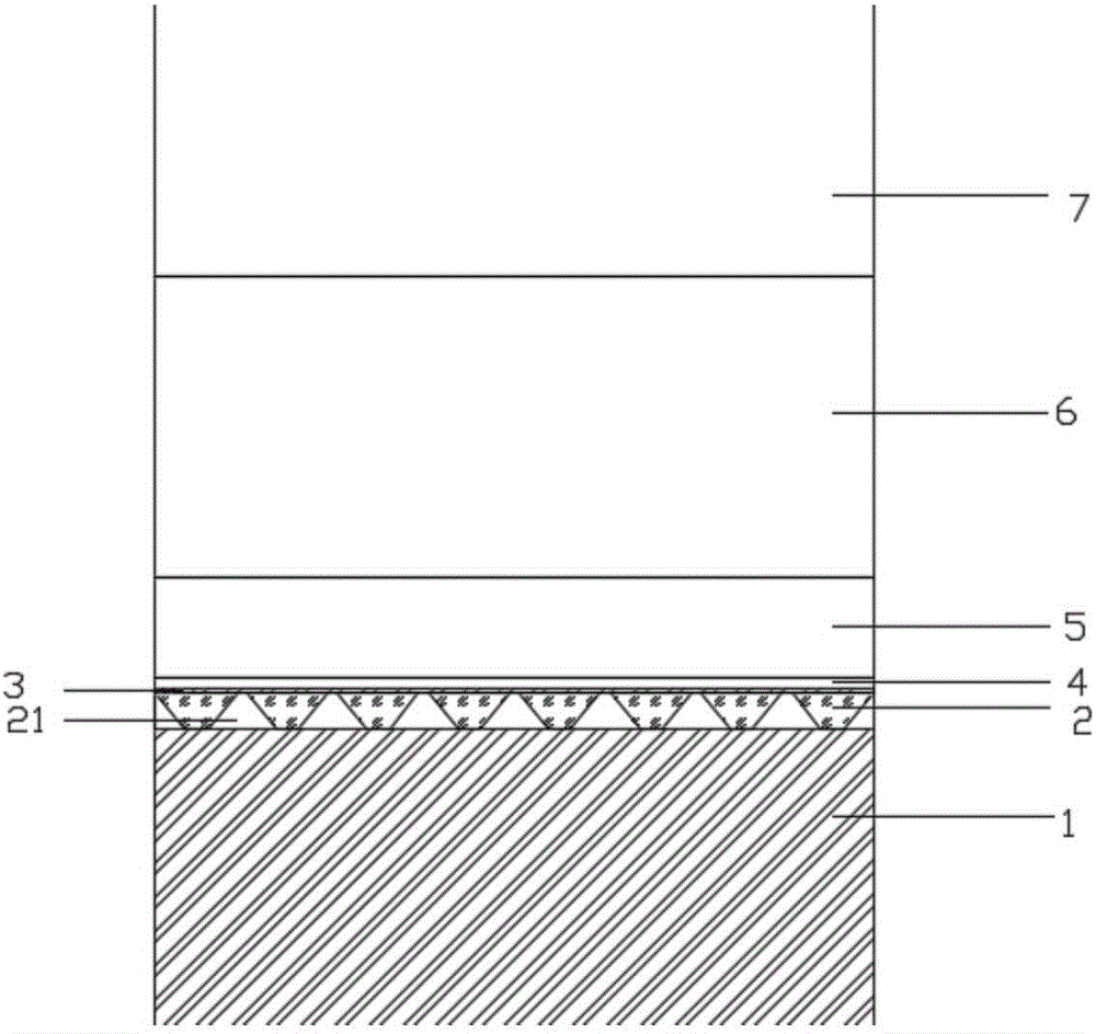
[0037] Step 102 : forming a concave layer 2 on the single crystal Si substrate 1 .

[0038] The formation process of the concave layer 2 is as follows: firstly, a SiO2 thin layer is formed on the surface of the single crystal Si substrate 1 by thermal oxidation, and ion implantation is performed through the SiO2 thin layer to prevent the single crystal Si substrate 1 from being polluted during the ion implantation process , high-energy ion implantation into Si, and then use HF to remove the SiO2 thin layer, and then selectively wet-etch the single-crystal Si substrate 1 after impl...

Embodiment 2

[0050] Step 101: Select a single crystal Si substrate 1 and clean the single crystal Si substrate 1 .

[0051] The crystal plane of the single crystal Si substrate 1 is the (100) crystal plane, which is an intrinsic type n-type silicon wafer with a thickness of 400 μm, and the growth of silicon is biased towards the (011) crystal plane by 4°.

[0052] Step 102 : forming a concave layer 2 on the single crystal Si substrate 1 .

[0053] The formation process of the concave layer 2 is as follows: firstly, Si ions are implanted into the single crystal Si substrate 1 with high-energy ions, and then the single crystal Si substrate implanted with Si ions is selectively dry etched to form the concave layers arranged in an array. The groove 21 constitutes the concave layer 2 and has a thickness of 90 nm.

[0054] Step 103 : forming a Si thin film layer 3 on the concave layer 2 , and the Si thin film layer 3 is suspended in the groove 21 of the concave layer 2 .

[0055] The Si thin f...


PUM

PropertyMeasurementUnit
thicknessaaaaaaaaaa
thicknessaaaaaaaaaa
temperatureaaaaaaaaaa

Abstract

The invention relates to the technical field of semiconductor manufacturing and design, and in particular relates to a GaAs/Si epitaxial material preparation method which comprises the following steps: selecting a single crystal Si substrate, and washing the single crystal Si substrate; forming a concave layer on the single crystal Si substrate; forming an Si film layer on the concave layer, and suspending the Si film layer in the groove of the concave layer; forming a GaAs seed layer on the Si film layer; forming a first GaAs buffer layer on the GaAs seed layer; forming a GaAs second buffer layer on the first GaAs buffer layer; and forming a GaAs epitaxial layer on the second GaAs buffer layer. By adopting the method, the high-quality GaAs crystal film can be prepared on the single crystal Si substrate which is low in price, and moreover an additional stress field is not introduced, so that additional adverse influence on quality of devices can be avoided in later device manufacturing.

Description

[0001] Technical field: [0002] The invention relates to the technical field of semiconductor manufacturing and design, in particular to a GaAs / Si epitaxial material preparation method. Background technique [0003] Due to its unique physical and chemical properties (direct band gap, band gap matching with the solar spectrum, high light absorption coefficient, etc.), GaAs thin films have attracted more and more attention. controlled sputtering, chemical vapor deposition, and molecular beam epitaxy. Due to the cheap Si material, mature technology, and large-diameter wafers, there are currently many applications based on Si materials. Silicon-based microelectronic devices continue to promote the rapid development of modern information technology. Epitaxial growth on Si-based GaAs thin film is beneficial to cost reduction and device integration. However, the lattice matching between GaAs and silicon materials is poor, and GaAs materials directly prepared on Si substrates will ...

Claims


Application Information

Patent Timeline
Patent Type & Authority Applications(China)
IPC IPC(8): C30B25/18C30B29/42H01L21/02
CPCC30B25/183C30B25/186C30B29/42H01L21/02381H01L21/0243H01L21/02463H01L21/02546
Inventor 王文庆
Owner DONGGUAN LIANZHOU INTPROP OPERATION MANAGEMENT CO LTD
Why Eureka
Try Eureka