
Light-emitting diode package structure manufacturing method
A technology of light-emitting diodes and packaging structures, applied in electrical components, circuits, semiconductor devices, etc., can solve the problems of high material cost and process cost
- Summary
- Abstract
- Description
- Claims
- Application Information
AI Technical Summary
Problems solved by technology
Method used
Image

Examples
Embodiment Construction
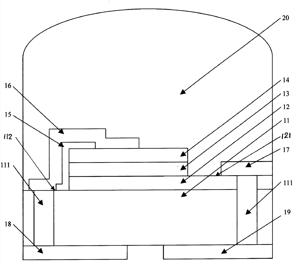
[0026] see figure 1 As shown, the present invention provides a method for manufacturing a light emitting diode packaging structure, comprising the following steps:
[0027] On an insulating substrate 11, the n-type layer 12, the active layer 13 and the p-type layer 14 are sequentially grown by metal-organic vapor phase epitaxy to form an epitaxial layer; wherein the material of the insulating substrate 11 is sapphire or silicon carbide or nitride Aluminum; wherein the n-type layer 12 and the p-type layer 14 in the epitaxial structure are upright or reversed. The material of the n-type layer 12 is n-type GaN, the material of the active layer 13 is a quantum well structure made of GaN material, and the material of the p-type layer 14 is p-type GaN.
[0028] The side above the p-type layer 14 is etched downward by a photolithography process, and the etching depth reaches the surface of the n-type layer 12 to form a first mesa 121, and the other side above the p-type layer 14 is ...
PUM
 Abstract
Description
Claims
Application Information