Electronic multiplying charge coupled device (CCD) sine wave driving method

A technology of sine wave drive and electron multiplication, applied in TV, electrical components, color TV, etc., can solve problems such as difficult debugging, difficult linear adjustment and control of amplitude and phase, achieve good versatility and practicability, and improve image quality , easy-to-achieve effects

Inactive Publication Date: 2011-11-02
BEIJING RES INST OF SPATIAL MECHANICAL & ELECTRICAL TECH
View PDF3 Cites 12 Cited by
  • Summary
  • Abstract
  • Description
  • Claims
  • Application Information

AI Technical Summary

Problems solved by technology

The advantage of this method is that the circuit form is simple and the energy consumption is small; the disadvantage is that the amplitude and phase are difficult to adjust and control linearly, and the debugging is difficult

Method used


Image

  • Electronic multiplying charge coupled device (CCD) sine wave driving method
  • Electronic multiplying charge coupled device (CCD) sine wave driving method
  • Electronic multiplying charge coupled device (CCD) sine wave driving method

Examples


Embodiment Construction

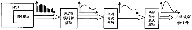
[0036] The present invention is realized through the following steps:

[0037] 1. Generate a sine wave code stream V composed of a set of normalized values ​​of N points 0 ,in i=0, 1, 2...N, N≧16.

[0038] 2. Convert the sine wave code stream V 0 After synchronizing with the timing signal Sig1 of the electron multiplier CCD, digital-to-analog conversion is performed to obtain a sine wave analog signal V 0 '.

[0039] 3. For sine wave analog signal V 0 'Perform low-pass filtering to obtain a smooth sine wave signal V 0 "."

[0040] 4. For smooth sine wave signal V 0 "Amplify to obtain the amplified sine wave drive signal V 0 "'.

[0041] 5. The amplified sine wave drive signal V 0 "' is compared with the drive signal Rφ1 obtained by the timing signal Sig1 of the electron multiplier CCD through the drive circuit to obtain the amplified sine wave drive signal V 0 The phase difference between "' and the drive signal Rφ1

[0042] 6. Send the amplified sine wave drive...


PUM


Abstract

The invention discloses an electronic multiplying charge coupled device (CCD) sine wave driving method. A series of adjustment is performed on a sine wave code stream to obtain relations between phase differences and CCD image data mean values, and an optimal phase difference is determined by a fitted curve to correct an initial sine wave code stream. In the method, rough adjustment and fine adjustment are performed on sine wave phases to obtain a relation curve for the phase differences and the CCD image data mean values, thereby determining the phase difference corresponding to a maximum CCD image data mean value to accurately correct sine waves to obtain an optimized electronic multiplying CCD driving signal and finally fulfill the aims of optimizing system imaging and improving imaging quality; and a direct-digital-synthesizer (DDS)-based digital/analogue hybrid circuit technology is adopted, and the linear amplification of the sine waves is realized by a high frequency high voltage amplification circuit.

Description

technical field [0001] The invention relates to an electron multiplication CCD sine wave driving method, which belongs to the technical field of electron multiplication CCD low-light imaging. Background technique [0002] Electron multiplication CCD is the core device of low-light imaging. Using the multiplication effect of electron multiplication CCD can eliminate the influence of readout noise, realize imaging in weak light environment, and even photon counting function. The realization of electron multiplication requires high-frequency and high-voltage (frequency ≥ 10MHz, voltage ≥ 50Vpp) driving signals. There are two existing driving methods: [0003] The first is the square wave drive method, such as figure 1 As shown, the low-voltage square wave is converted into a square-wave drive signal through the high-voltage buffer, and the signal amplitude is determined by the high-voltage power supply. At the same time, in order to ensure the stability of the amplitude, the ...

Claims


Application Information

Patent Timeline
Patent Type & Authority Applications(China)
IPC IPC(8): H04N5/341H04N5/351
Inventor 张玉贵何志宽王磊韩志学卜洪波董长哲
Owner BEIJING RES INST OF SPATIAL MECHANICAL & ELECTRICAL TECH
Why Eureka
Try Eureka