Epitaxial growth method of InGaN quantum dot and single photon source obtained thereby

A technology of epitaxial growth and growth method, which is applied in the field of single photon source, can solve the problems of large randomness of InGaN quantum dots, difficult control of lateral size and density, unsuitability for single photon source, etc., to achieve suitable for large-scale application, mild conditions, The effect of simple steps

Inactive Publication Date: 2011-11-16
TSINGHUA UNIV
View PDF2 Cites 13 Cited by
  • Summary
  • Abstract
  • Description
  • Claims
  • Application Information

AI Technical Summary

Problems solved by technology

InGaN quantum dots grown by the current method are highly random, and their lateral size and density are not easy to control, so they are not suitable for use as a single photon source.

Method used


Image

  • Epitaxial growth method of InGaN quantum dot and single photon source obtained thereby
  • Epitaxial growth method of InGaN quantum dot and single photon source obtained thereby
  • Epitaxial growth method of InGaN quantum dot and single photon source obtained thereby

Examples


Embodiment 1

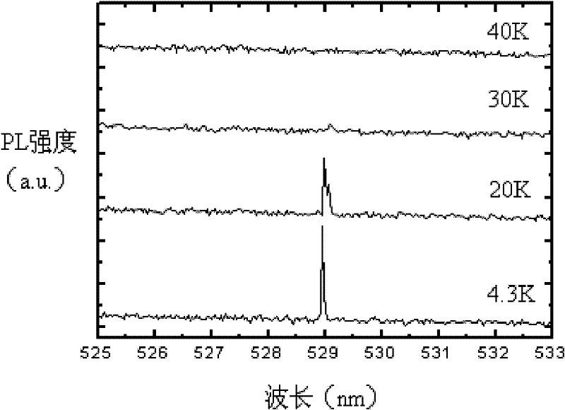
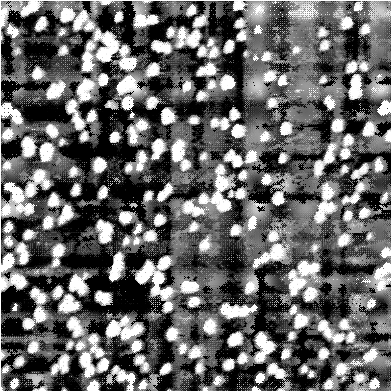
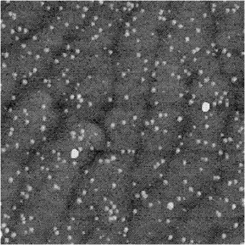
[0031] Using MOCVD to grow low-density InGaN quantum dots in the low-temperature GaN insertion layer, the epitaxy sequence is as follows Figure 4 As shown, its specific growth process is:

[0032] 1. The carrier gas is H 2 , the sapphire substrate at H 2 Cleaning was carried out for 10 minutes under ambient conditions, the temperature was 1060° C., and the pressure of the reaction chamber was 200 mbar.

[0033] 2. The carrier gas is H 2 , a 30nm-thick GaN buffer layer was grown on a sapphire substrate at a temperature of 530°C and a reaction chamber pressure of 400mbar.

[0034] 3. The carrier gas is H 2 , a GaN bulk material with a thickness of 2 μm was grown on the GaN buffer layer at a temperature of 1040° C. and a reaction chamber pressure of 400 mbar.

[0035] 4. Switch the carrier gas to N 2 , grow a 20nm-thick GaN insertion layer on the GaN bulk material at a temperature of 650°C and a reaction chamber pressure of 400mbar.

[0036] 5. The carrier gas is N 2 , I...

Embodiment 2

[0040]Using MOCVD to grow low-density InGaN quantum dots in the low-temperature GaN insertion layer, the epitaxy sequence is as follows Figure 4 As shown, its specific growth process is:

[0041] 1. The carrier gas is H 2 , SiC substrate in H 2 Cleaning was carried out for 10 minutes under ambient conditions, the temperature was 1200° C., and the pressure of the reaction chamber was 400 mbar.

[0042] 2. The carrier gas is H 2 , a 20nm-thick AlN buffer layer was grown on a SiC substrate at a temperature of 1200°C and a reaction chamber pressure of 100mbar.

[0043] 3. The carrier gas is H 2 , a 2000nm thick GaN bulk material was grown on the AlN buffer layer at a temperature of 1100°C and a reaction chamber pressure of 400mbar.

[0044] 4. Switch the carrier gas to N 2 , a 25nm-thick GaN insertion layer was grown on the GaN bulk material at a temperature of 765°C and a reaction chamber pressure of 400mbar.

[0045] 5. The carrier gas is N 2 , grow InGaN quantum dots o...

Embodiment 3

[0049] Using MOCVD to grow multi-layer low-density InGaN quantum dots in the low-temperature GaN insertion layer to form a single photon source of multi-layer quantum dot mechanism, the epitaxial growth sequence is as follows Figure 5 As shown, its specific growth process is:

[0050] 1. The carrier gas is H 2 , the sapphire substrate at H 2 Cleaning was carried out for 10 minutes under ambient conditions, the temperature was 1060° C., and the pressure of the reaction chamber was 200 mbar.

[0051] 2. The carrier gas is H 2 , a 50nm-thick AlN buffer layer was grown on a sapphire substrate at a temperature of 400°C and a reaction chamber pressure of 400mbar.

[0052] 3. The carrier gas is H 2 , a 5 μm thick GaN bulk material was grown on the AlN buffer layer at a temperature of 1040° C. and a reaction chamber pressure of 400 mbar.

[0053] 4. Switch the carrier gas to N 2 , a 15nm-thick GaN insertion layer was grown on the GaN bulk material at a temperature of 650°C and a...


PUM


Abstract

The invention relates to an epitaxial growth method of an InGaN quantum dot. The method comprises the following steps: growing a low-temperature buffer layer, a high-temperature GaN body material and a low-temperature GaN insertion layer on a substrate in an epitaxial way; and then growing an InGaN quantum dot on the GaN insertion layer in an epitaxial way. The invention also provides an InGaN quantum dot single photon source which is obtained by using the epitaxial growth method. The quantum dot obtained by using the epitaxial growth method provided by the invention has high quantum confinement effect, and is very suitable for manufacturing a single photon source; and the epitaxial growth method can reduce the horizontal size and density of the quantum dot effectively and has simple and convenient steps, moderate conditions and wide application value.

Description

technical field [0001] The invention relates to the field of semiconductor materials, in particular to an epitaxial growth method of low-density InGaN quantum dots and the obtained single photon source containing the low-density InGaN quantum dots. Background technique [0002] Due to the quantum confinement effect of three-dimensional space, InGaN quantum dots have potential wide application in optoelectronic devices such as semiconductor light-emitting diodes and single photon sources, and the low-dimensional structure of quantum dots will produce some novel physical phenomena such as double exciton transition phenomena, etc. , so the research on InGaN quantum dots has attracted much attention. [0003] At present, the preparation of InGaN quantum dots mainly adopts self-assembly growth technology, and the transformation from two-dimensional growth mode to three-dimensional growth mode is realized on GaN by using stress induction. The published results are: [0004] 1. G...

Claims


Application Information

Patent Timeline
Patent Type & Authority Applications(China)
IPC IPC(8): H01L33/00H01L33/04
Inventor 罗毅吕文彬汪莱郝智彪
Owner TSINGHUA UNIV
Why Eureka
Try Eureka