White light LED (light emitting diode) encapsulation structure and method

A technology of LED encapsulation and encapsulation method, which is applied in the direction of electrical components, electric solid devices, circuits, etc., can solve the problems of uneven coating amount of phosphor powder coating, improve uniformity and luminous efficiency, improve color consistency, The effect of prolonging life

Inactive Publication Date: 2013-02-13
HARBIN INST OF TECH
View PDF6 Cites 0 Cited by
  • Summary
  • Abstract
  • Description
  • Claims
  • Application Information

AI Technical Summary

Problems solved by technology

[0005] The present invention aims to solve the problem of uneven coating amount of the fluorescent powder coating of the current white light LED, and provides a white light LED packaging structure and packaging method

Method used


Image

  • White light LED (light emitting diode) encapsulation structure and method
  • White light LED (light emitting diode) encapsulation structure and method
  • White light LED (light emitting diode) encapsulation structure and method

Examples


specific Embodiment approach 1

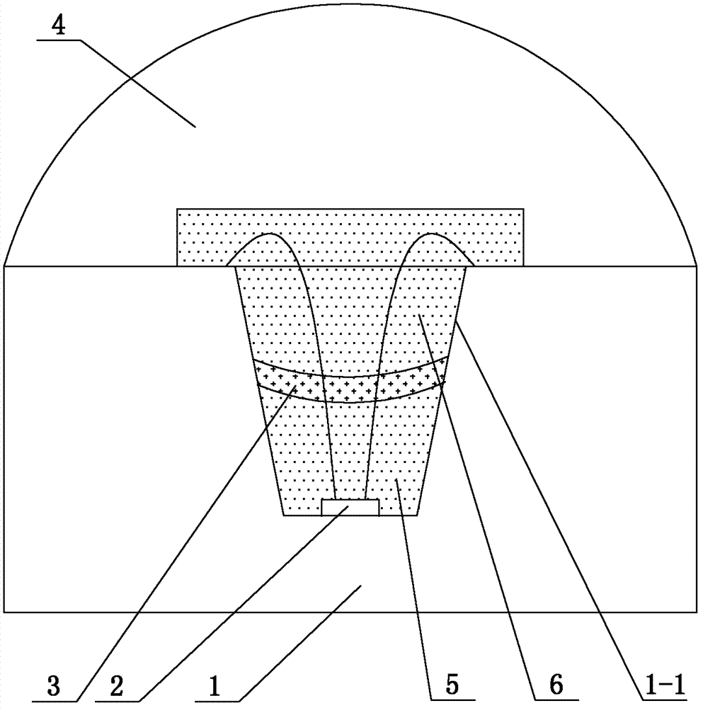
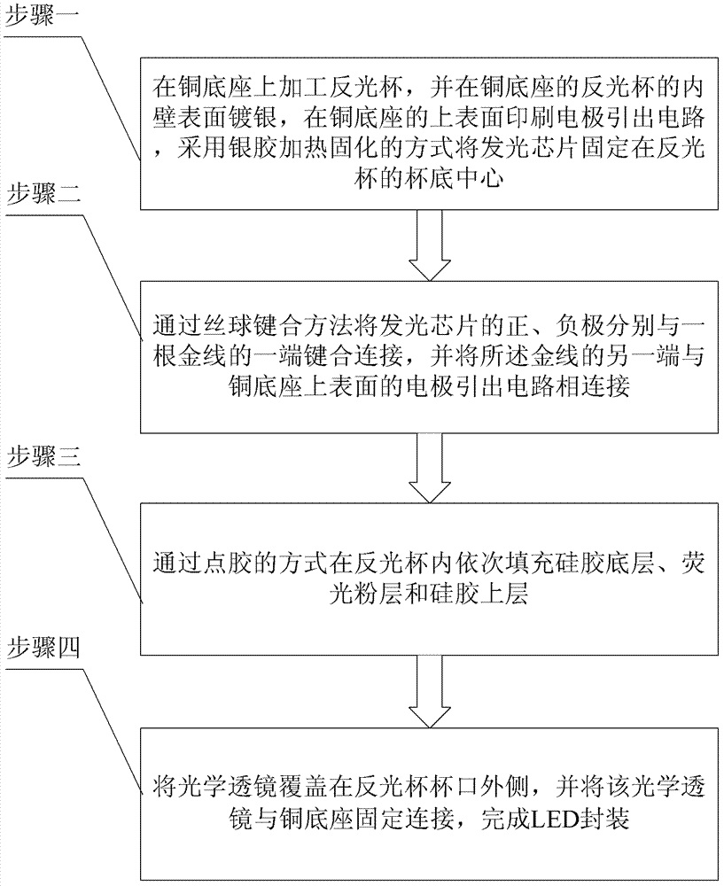
[0028] Specific implementation mode one: the following combination figure 1 Describe this embodiment mode, the white light LED package structure described in this embodiment mode, it comprises copper base 1, light-emitting chip 2, phosphor layer 3 and optical lens 4, it also comprises silica gel bottom layer 5 and silica gel upper layer 6,

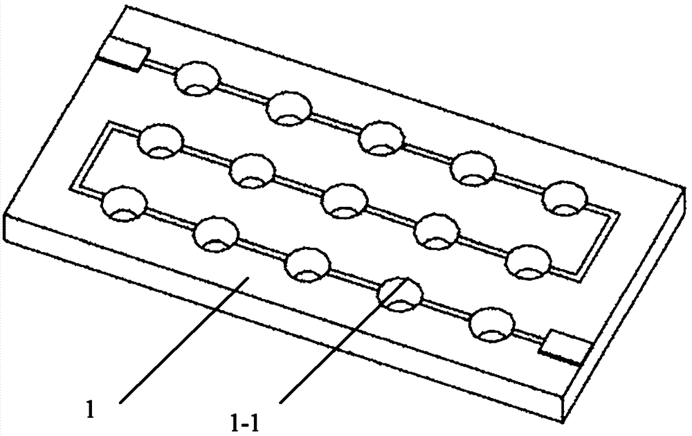
[0029] The center of the copper base 1 has a concave reflective cup 1-1, the inner wall surface of the reflective cup 1-1 is plated with silver, the center of the bottom of the reflective cup 1-1 is fixed with the light-emitting chip 2, and the upper surface of the copper base 1 is printed with an electrode lead-out circuit , the positive and negative plates of the light-emitting chip 2 are respectively connected to the electrode lead-out circuit through gold wires for ball bonding,

[0030] The bottom of the reflective cup 1-1 is filled with silica gel bottom layer 5 to fix the light-emitting chip 2, the upper surface of the reflective cu...

specific Embodiment approach 2

[0033] Embodiment 2: This embodiment is a further description of Embodiment 1. The light-emitting chip 2 is fixed at the center of the bottom of the reflective cup 1-1 by heating and curing silver glue.

specific Embodiment approach 3

[0034] Embodiment 3: This embodiment is a further description of Embodiment 1 or 2. The electrode lead-out circuit is realized by a printed conductive silver paste layer, and an insulating ink printing layer is between the conductive silver paste layer and the copper base 1 .

[0035] In this embodiment, the conductive silver paste layer is used to realize the electrode lead-out circuit, and the copper base 1 is conducive to better heat dissipation.


PUM


Abstract

The invention discloses a white light LED (light emitting diode) encapsulation structure and method, belonging to the technical field of LED encapsulation. Through the invention, the problem of non-uniform coating weight of the fluorescent powder coating of the existing white light LED is solved. The encapsulation structure disclosed by the invention is characterized in that: an inward-concave light reflecting cup is arranged at the center of a copper base; silver is plated on the surface of the inner wall of the light reflecting cup; a luminous chip is fixed at the center of the bottom of the light reflecting cup; an electrode leading-out circuit is printed on the upper surface of the copper base; the positive and negative plates of the luminous chip are connected with the electrode leading-out circuit by use of gold wires through wire ball bonding respectively; the bottom of the light reflecting cup is sequentially filled with a silica gel bottom layer, a fluorescent powder layer and a silica gel upper layer through dispensing; and an optical lens covers and is fixed on the mouth of the light reflecting cup on the upper surface of the copper base. In the encapsulation method disclosed by the invention, a silica gel bottom layer is added between the fluorescent powder layer and the luminous chip so that a distance between the fluorescent powder layer and the luminous chip is relatively controllable and the coating of the fluorescent powder layer is more uniform. The encapsulation method and structure disclosed by the invention are suitable for encapsulating LEDs.

Description

technical field [0001] The invention relates to a white light LED packaging structure and packaging method, belonging to the technical field of LED packaging. Background technique [0002] LED is called the fourth-generation lighting source or green light source. It has the characteristics of energy saving, environmental protection, long life and small size. It is widely used in various indications, displays, decorations, backlights, general lighting and urban night scenes. [0003] At present, the process of realizing white light of LED is to coat YAG phosphor on the blue chip, use the blue light of the blue chip to excite the phosphor to emit yellow-green light, and then synthesize white light with the blue light of the blue chip itself. The process of coating YAG phosphor on the blue chip is usually: mix the phosphor with glue, and then apply it to the blue chip with a dispenser and heat it to cure. This implementation method is relatively simple, efficient and practical...

Claims


Application Information

Patent Timeline
Patent Type & Authority Patents(China)
IPC IPC(8): H01L33/52H01L33/00
CPCH01L2224/45144H01L2224/48091
Inventor 杭春进王春青
Owner HARBIN INST OF TECH
Why Eureka
Try Eureka