Selected area polymer bonded-silicon-based mixing laser and manufacturing method thereof

A technology of mixing lasers and polymers, applied in lasers, laser parts, semiconductor lasers, etc., can solve the problems of poor practicability, low output power, and low coupling efficiency, and achieve simple operation, low cost, and environmental requirements. high effect

Inactive Publication Date: 2011-11-16
PEKING UNIV
View PDF3 Cites 8 Cited by
  • Summary
  • Abstract
  • Description
  • Claims
  • Application Information

AI Technical Summary

Problems solved by technology

Therefore, this scheme has the disadvantages of low output power and poor practicability
[0004] Therefore, the current polymer-bonded silicon-based hybrid lasers have the disadvantages of low coupling efficiency, low output power, and poor practicability

Method used


Image

  • Selected area polymer bonded-silicon-based mixing laser and manufacturing method thereof
  • Selected area polymer bonded-silicon-based mixing laser and manufacturing method thereof
  • Selected area polymer bonded-silicon-based mixing laser and manufacturing method thereof

Examples


Embodiment Construction

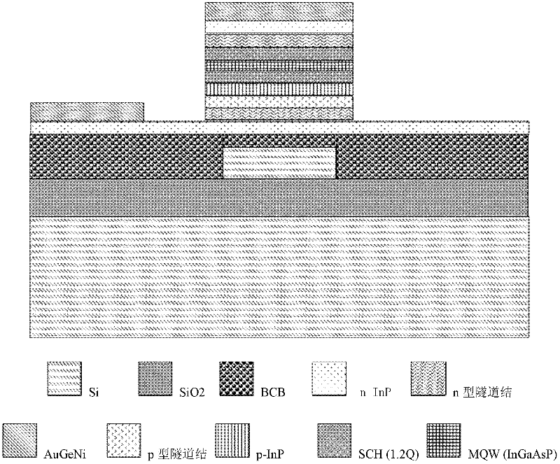
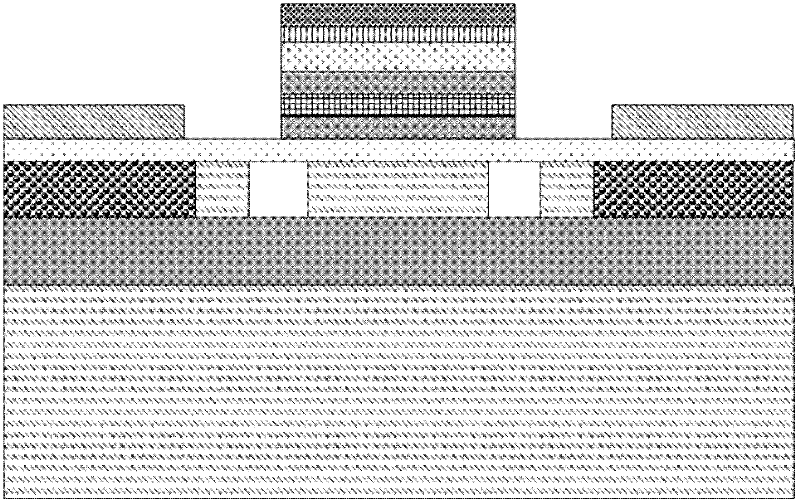
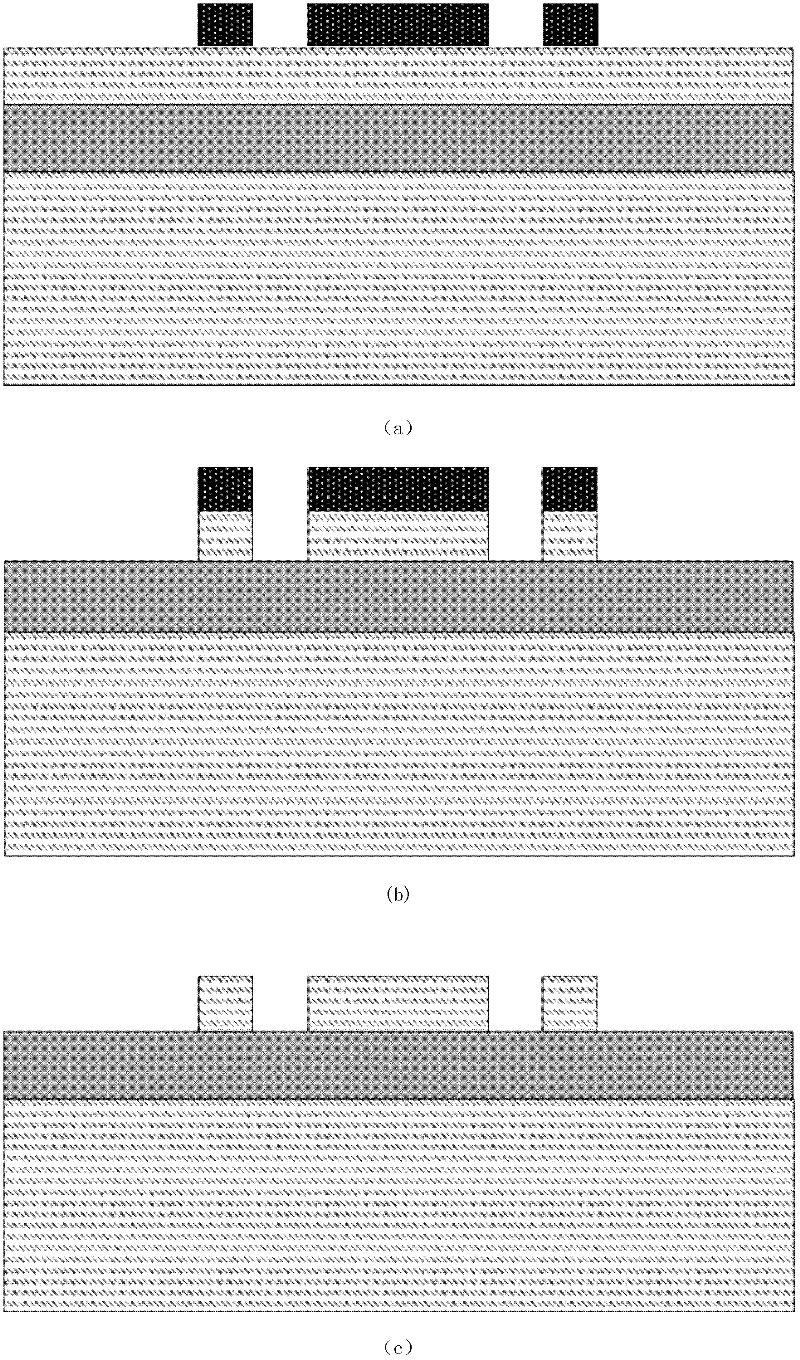
[0025] Combine below image 3 , taking the InP laser as an example to further describe the present invention in detail:

[0026] 1. Put a layer of photoresist on the SOI silicon wafer, and use a photolithography plate with a periodic structure for photolithography, development, and fixation. like image 3 (a) shown.

[0027] 2. Use ICP etching to etch away the Si not covered by the photoresist until the Si waveguide, bonding area and Si barrier wall are etched, and a silicon barrier wall is etched between the silicon waveguide and the bonding area. The goal is to prevent the polymer from flowing into the silicon waveguide during bond pressing, affecting the coupling of light from the laser into the silicon waveguide. The height of the Si waveguide and the barrier wall are both 800nm, the width of the waveguide is 3μm, and the width of the barrier wall is 1μm, such as image 3 (b) shown.

[0028] 3. Remove photoresist, such as image 3 (c) shown.

[0029] 4. Spin-coat a ...


PUM

PropertyMeasurementUnit
thicknessaaaaaaaaaa
refractive indexaaaaaaaaaa

Abstract

The invention discloses a selected area polymer bonded-silicon-based mixing laser and a manufacturing method thereof, belonging to the field of silicon-based electronic devices. The laser comprises an SOI (silicon on insulator) layer on which a bonded area and an optical coupling area are etched, wherein the SOI layer is provided with a multiregion layer; a bonding polymer, a silicon barrier wall, an air gap, a silicon waveguide, an air gap, a silicon barrier wall and a bonding polymer are arranged in the multiregion layer sequentially from left to right; the multiregion layer is provided with an n-type III-V group material layer; a multilayer structure is arranged at a position corresponding to the silicon waveguide on the n-type III-V group material layer; the multilayer structure comprises a first SCH (separate confinement heterostructure) layer, an MQW (multiple quantum well) layer, a second SCH layer, a p-type III-V group material layer, a p-type etching barrier layer and a p-type ohmic contact layer in sequence from top to bottom; and ohmic contact layers made of n-type III-V group materials are arranged at the left and right sides of the multilayer structure on the n-type III-V group material layer respectively. The laser can be applied to monolithic-silicon-based optoelectronic integration as a silicon-based light source, and is easy to manufacture and low in cost.

Description

technical field [0001] The invention relates to a hybrid silicon-based laser device and a preparation method thereof in the field of silicon-based optoelectronic devices, in particular to an area-selective polymer-bonded silicon-based hybrid laser and a preparation method thereof. Background technique [0002] In today's information society, in order to further improve the computing speed and information storage capacity of electronic computers, people imagine using photons instead of electrons as information carriers. The propagation speed of photons is fast, the bandwidth is several orders of magnitude larger than that of electrons, and it has the advantages of fast response speed, large transmission capacity, fast processing speed, integration and high resistance to electromagnetic interference. Therefore, people hope to combine photon technology with silicon microelectronics. The combination of technologies realizes silicon-based optoelectronic integration. One of the k...

Claims


Application Information

Patent Timeline
Patent Type & Authority Applications(China)
IPC IPC(8): H01S5/22H01S5/323
Inventor 秦国刚洪涛李艳平冉广照陈娓兮
Owner PEKING UNIV
Why Eureka
Try Eureka