Sapphire wafer dividing method

A sapphire wafer and sapphire technology, applied in stone processing equipment, fine working devices, laser welding equipment, etc., can solve the problems of obstructing laser line irradiation, unable to form a modified layer, etc., and achieve the effect of improving the manufacturing yield

Active Publication Date: 2011-11-23
DISCO CORP
View PDF5 Cites 14 Cited by
  • Summary
  • Abstract
  • Description
  • Claims
  • Application Information

AI Technical Summary

Problems solved by technology

However, since the reflective film is formed on the surface opposite to the surface on which the active layer is formed, there is a problem t

Method used


Image

  • Sapphire wafer dividing method
  • Sapphire wafer dividing method
  • Sapphire wafer dividing method

Examples


Embodiment Construction

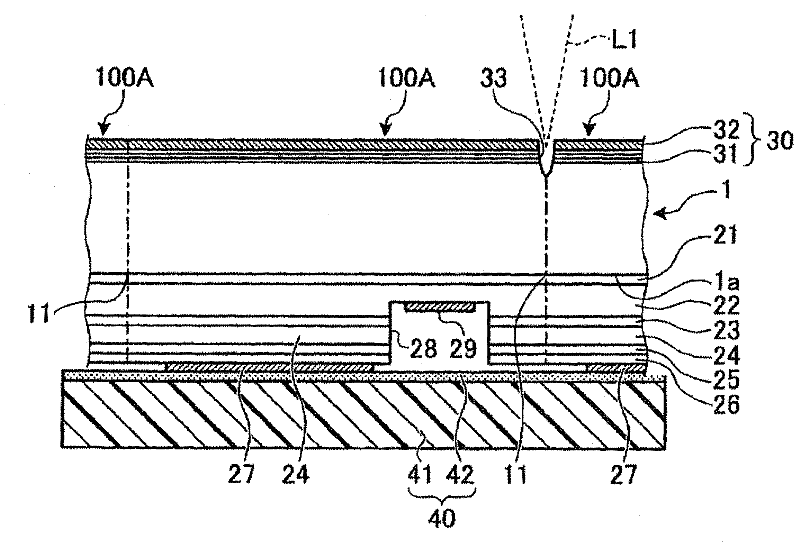
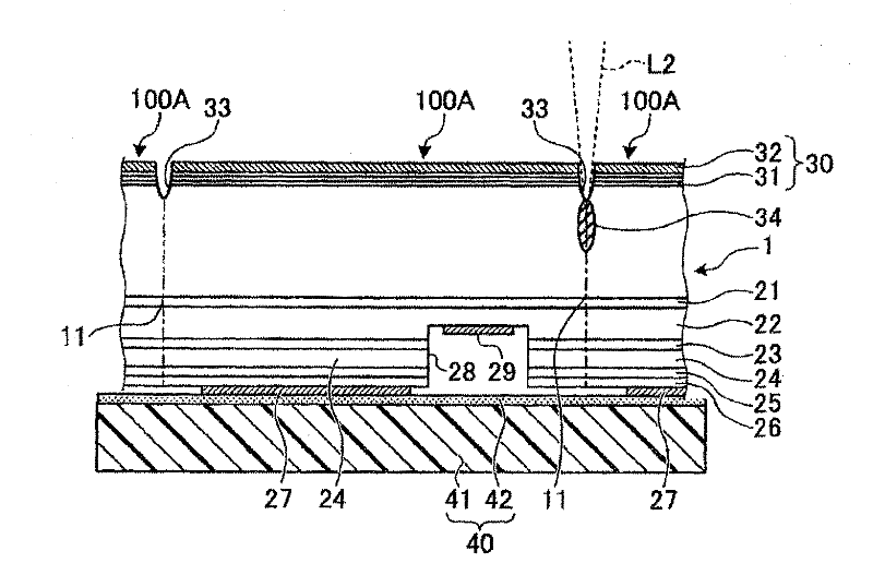
[0016] Hereinafter, a method for dividing a sapphire wafer according to an embodiment of the present invention will be described in detail with reference to the drawings. It should be noted that the drawings are only schematic illustrations, and the thickness and thickness ratio of each layer are different from actual ones. In addition, in the method of dividing a sapphire wafer according to the present embodiment, a wafer in which a semiconductor layer, a reflective film, and the like are formed on a sapphire wafer to form a light-emitting element as a light-emitting device is used as an object of division.

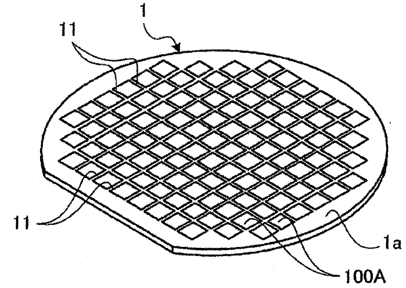
[0017] Here, as an example of a sapphire wafer to which the dividing method according to the embodiment of the present invention is applied, Figure 1 ~ Figure 3 A sapphire wafer 1 is shown for illustration. like figure 1 As shown, in this sapphire wafer 1 , light-emitting element portions 100A are formed in respective regions of the front surface 1 a of the sapphire w...


PUM


Abstract

The invention provides a sapphire wafer dividing method, capable of performing a precise division processing to the sapphire wafer provided with a reflection film. A pulse laser absorbed by a reflection film 30 is illuminated from the back face side of the sapphire wafer 1 along a division predetermining line 11 in a convergence way; a groove 33 deeper than the reflection film 30 is formed on the division predetermining line 11; then the pulse laser L2 transmitting through the sapphire is illuminated inside the sapphire wafer 1 in the convergence way along the division predetermining line 11 passing through the groove 33 and exposed out of the sapphire surface; a modification layer 34 is formed inside; an external force is applied to the modification layer 34 so as to divide the sapphire wafer 1 along the division predetermining line 11.

Description

technical field [0001] The present invention relates to a sapphire wafer dividing method for dividing a sapphire wafer in which light-emitting devices having reflective films are respectively formed in a plurality of element formation regions along planned dividing lines. Background technique [0002] As a light-emitting device manufactured using a sapphire wafer, there is a light-emitting diode (LED) in which a nitride semiconductor such as gallium nitride (GaN) is laminated on a sapphire substrate. Such light-emitting devices are respectively formed in element formation regions of the sapphire wafer surrounded by dividing lines. The sapphire wafer in which the light-emitting devices are respectively formed in the element formation regions is divided along the planned division lines, whereby individual light-emitting devices are obtained. [0003] However, since a sapphire wafer has a high Mohs hardness, it is difficult to divide it by a dicing device having a cutting blad...

Claims


Application Information

Patent Timeline
IPC IPC(8): B28D5/04B23K26/00B23K26/064B23K26/364B23K26/40B28D5/00H01L21/301H01L33/32
Inventor 星野仁志
Owner DISCO CORP
Why Eureka
Try Eureka