Lighting dose real-time controlling apparatus in photolithography system

A real-time control and lithography system technology, applied in the semiconductor field, can solve problems such as difficulty in building models, difficulty in long-term guarantee of accuracy, inability to test all exposure conditions, etc., to achieve the effect of improving accuracy

Inactive Publication Date: 2011-11-23
SHANGHAI MICRO ELECTRONICS EQUIP (GRP) CO LTD
View PDF6 Cites 18 Cited by
  • Summary
  • Abstract
  • Description
  • Claims
  • Application Information

AI Technical Summary

Problems solved by technology

This method has significant disadvantages. First, the optical system behind the energy sensor ED is very complex, including the uniform light system and objective lens, etc., and it is difficult to establish a correct model; second, in the measurement and calibration of model parameters, all exposure conditions cannot be These tests consume a lot of time, a

Method used


Image

  • Lighting dose real-time controlling apparatus in photolithography system
  • Lighting dose real-time controlling apparatus in photolithography system
  • Lighting dose real-time controlling apparatus in photolithography system

Examples


Embodiment 1

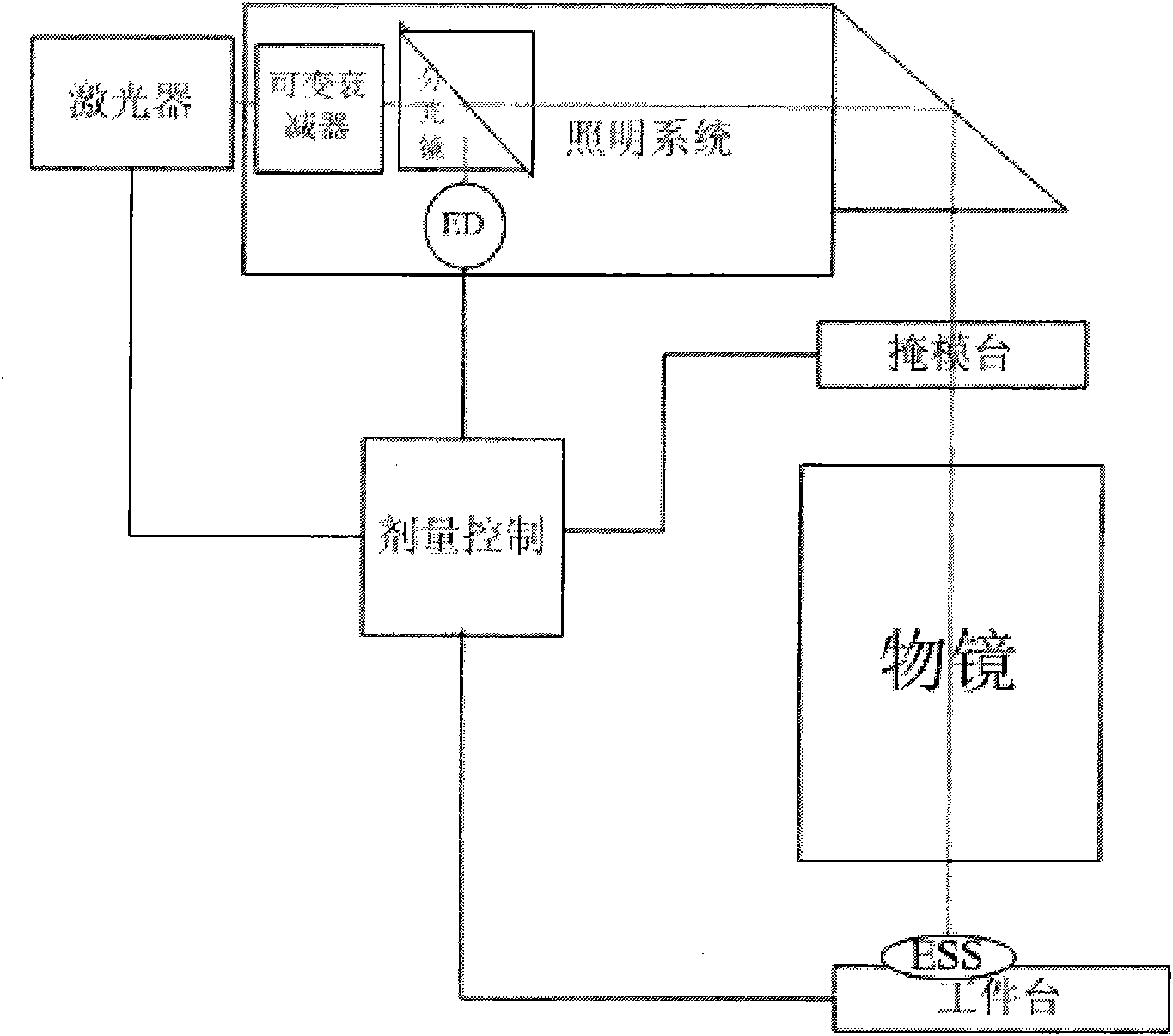
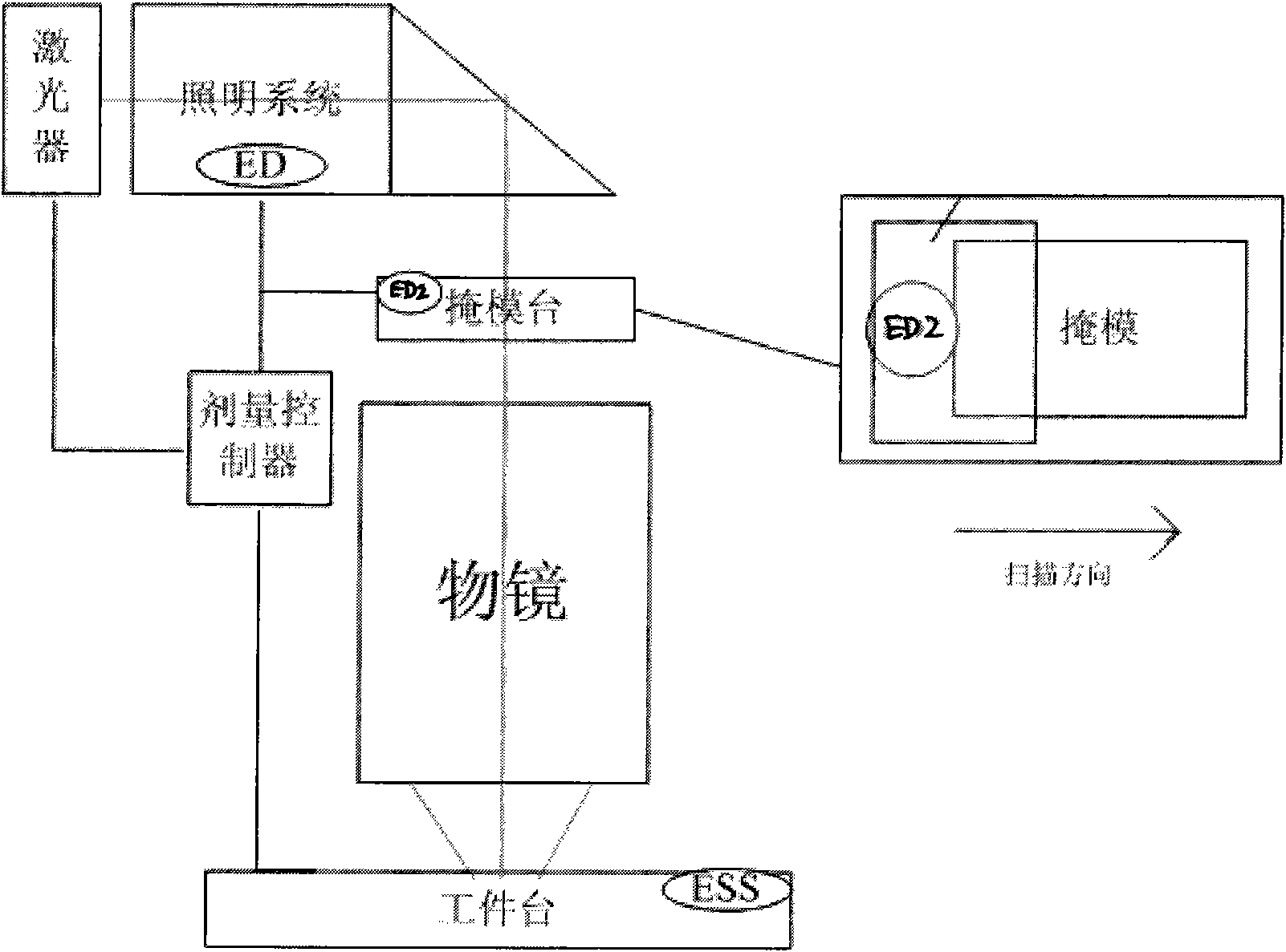
[0020] On the basis of the technical solution described in the background art, an energy sensor ED2 is added to the mask table above the objective lens of the lithography system, which is called the third light energy sensor. The point energy sensor ESS and energy sensor ED mentioned in the background art, They are respectively called the second light energy sensor and the first light energy sensor. Such as figure 2 , the energy sensor ED2 is installed on the center line of the mask stage in the scanning direction, on one side of the mask, adjacent to the mask. During each scanning exposure, the variable slit of synchronous scanning in the illumination system is opened earlier, or closed later, so that the illumination light also scans the energy sensor ED2 before or after scanning the mask; The energy sensor ED2 measures the energy of the pulse, and the pulse energy of the silicon plane can be calculated by multiplying the pulse energy measured by the energy sensor ED2 by t...

Embodiment 2

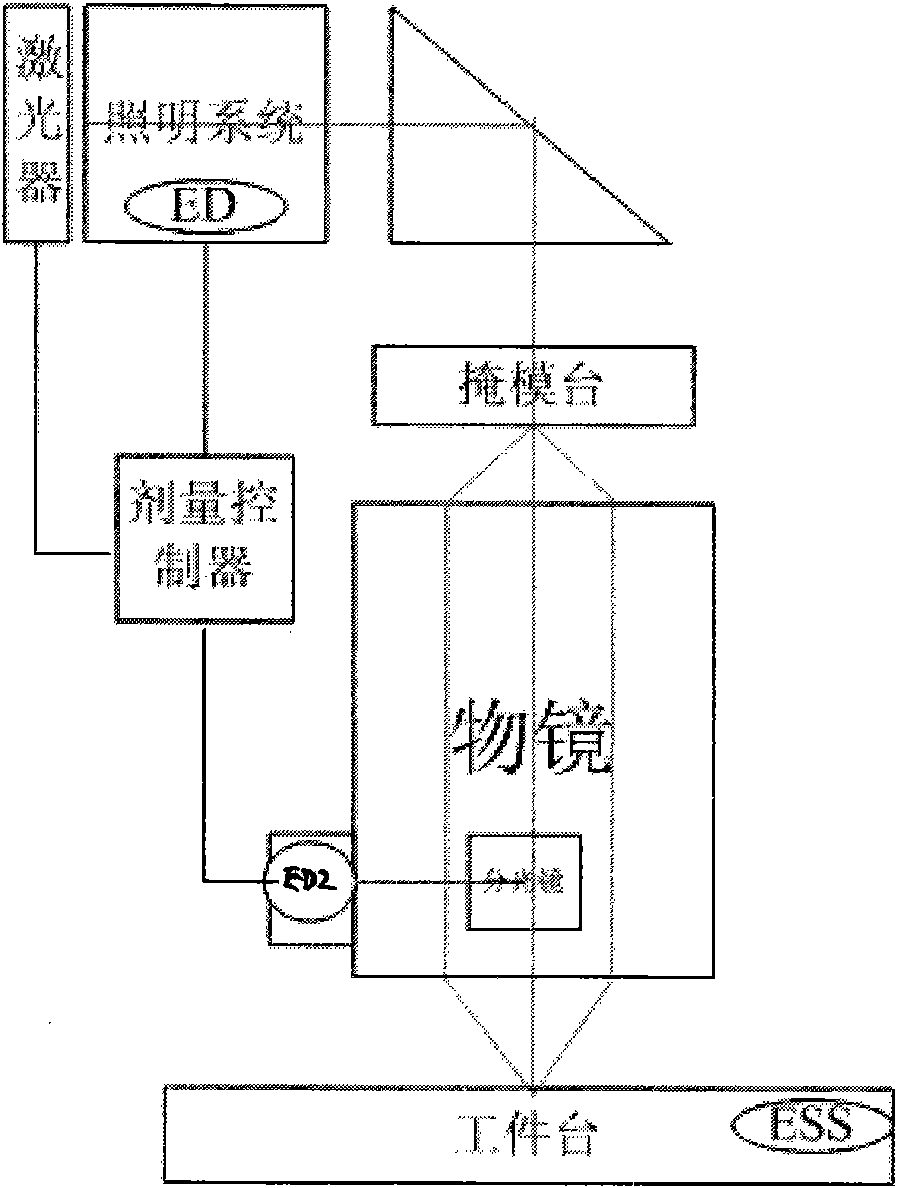
[0029] On the basis of the technical solution described in the background technology, an energy sensor ED2 is added inside the objective lens of the lithography system, which is called the third light energy sensor. The point energy sensor ESS and energy sensor ED mentioned in the background technology are respectively called the first light sensor. Two light energy sensors and a first light energy sensor. Such as image 3 , the energy sensor ED2 is installed on the upper side of the last lens inside the objective lens, and there is a beam splitter inside the objective lens to reflect the diffracted light inside the objective lens to the energy sensor ED2. Because the beam splitter only decomposes a small part of the light in the pupil, it does not affect the imaging and has little effect on the image quality. No matter how the illumination settings are changed, the diffracted light from the mask can always irradiate the beam splitter and be reflected by the beam splitter to ...

Embodiment 3

[0038] On the basis of the technical solution described in the background technology, an energy sensor ED2 is added below the objective lens of the lithography system away from the focal plane, which is called the third light energy sensor. The point energy sensor ESS and energy sensor ED mentioned in the background technology, They are respectively called the second light energy sensor and the first light energy sensor. Such as Figure 4 , the energy sensor ED2 is installed on the side below the last lens inside the objective lens, and there is a beam splitter under the objective lens away from the focal plane, which reflects the diffracted light under the objective lens to the energy sensor ED2. Because the beam splitter only decomposes a small part of the light away from the focal plane, it does not affect the imaging and has little impact on the image quality. No matter how the illumination setting is changed, the diffracted light from the mask can always be irradiated on...


PUM


Abstract

The invention discloses a lighting dose real-time controlling apparatus. The apparatus comprises orderly arranged components along an optical axis, which are: a light source, a lighting system, a mask bench, an object lens, and a workpiece bench. A first light energy detector and a second energy spot sensor are respectively arranged in the lighting system and on the workpiece bench. The apparatus is characterized in that: a third light energy detector is arranged in the light path between the first light energy detector and a second light energy spot sensor. The third light energy detector is used for measuring the lighting dose in real time during exposure. With the apparatus provided by the invention, light intensity between the first light energy detector and a second light energy spot sensor can be measured in real time during exposure, such that a yield is not influenced. The third light energy detector is arranged between the first light energy detector and a second light energy spot sensor, such that an influence of varied optics transmissivities between a first and a third light energy detectors is avoided. Therefore, a complicated transmissivity prediction model is not required. An accurate energy measured on a silicon surface can be obtained through simple reforming. Dose controlling can be carried out upon exposure fields according to the measuring results, such that dose accuracy can be improved.

Description

technical field [0001] The invention relates to the technical field of semiconductors, in particular to a device and method for real-time measurement and precise control of illumination dose in a photolithography system. Background technique [0002] Generally speaking, in the lithography machine system, there are two light energy sensors related to dose control. One is on the workpiece table, which is called Energy Spot Sensor (ESS for short), which is used to measure the visual field during non-exposure. Field profile and dose, one inside the lighting system, called Energy Detector, ED for short. Generally, the energy difference between laser pulses is relatively large, so the energy sensor ED is used to measure the beam energy in real time, and then perform real-time feedback control on the dose based on the measured value, such as figure 1 shown. [0003] The method of using the energy sensor ED for feedback control of the dose is to use the energy sensor ED to measure...

Claims


Application Information

Patent Timeline
IPC IPC(8): G03F7/20
Inventor 张俊
Owner SHANGHAI MICRO ELECTRONICS EQUIP (GRP) CO LTD
Why Eureka
Try Eureka