Etching method for improving power of light-transmitting solar cell module
A technology of battery components and solar thin films, which is applied in the direction of electrical components, circuits, semiconductor devices, etc., can solve the problems of affecting the electrical characteristics of batteries, affecting the output power of components, and increasing the number of defects, so as to reduce the cost of unit power generation, reduce leakage, Ensure the effect of light transmission performance
- Summary
- Abstract
- Description
- Claims
- Application Information
AI Technical Summary
Problems solved by technology
Method used
Image
Examples
Embodiment 1
[0025] The method for improving the power of the light-transmitting component by optimizing the scribing method includes the following steps:
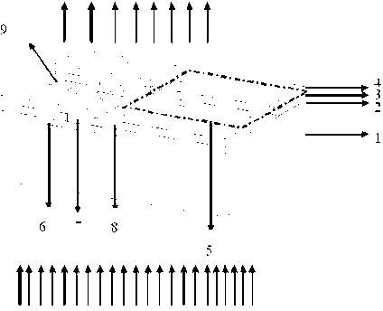
[0026] a. see figure 1: Utilize low-pressure chemical vapor deposition technology or magnetron sputtering technology to deposit transparent conductive film on the insulating substrate 1 float glass as the front electrode of the battery, the first transparent conductive electrode layer 2; then use plasma chemical vapor deposition technology (PECVD ) Deposit thin-film silicon p-i-n or p-i-n / p-i-n laminate structure and triple-junction silicon-based film structure on the coated glass substrate, photoelectric conversion layer 3; use low-pressure chemical vapor deposition technology to grow transparent conductive film on the above photoelectric conversion layer as a battery The back electrode is the second transparent conductive electrode layer 4 .
[0027] b. see figure 1 : In this embodiment, laser scribing is used to scribe the linear ...
Embodiment 2
[0034] The method for improving the power of the light-transmitting component by optimizing the scribing method includes the following steps:
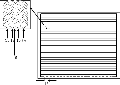
[0035] a. see figure 1 : Utilize low-pressure chemical vapor deposition technology or magnetron sputtering technology to deposit transparent conductive film on the insulating substrate 1 float glass as the front electrode of the battery, the first transparent conductive electrode layer 2; then use plasma chemical vapor deposition technology (PECVD ) Deposit thin-film silicon p-i-n or p-i-n / p-i-n laminate structure and triple-junction silicon-based film structure on the coated glass substrate, photoelectric conversion layer 3; use low-pressure chemical vapor deposition technology to grow transparent conductive film on the above photoelectric conversion layer as a battery The back electrode is the second transparent conductive electrode layer 4 .
[0036] b. see figure 2 Enlarged picture in the middle: In this embodiment, laser scribi...
PUM
| Property | Measurement | Unit |
|---|---|---|
| wavelength | aaaaa | aaaaa |
Abstract
Description
Claims
Application Information
 - R&D
- Intellectual Property
- Life Sciences
- Materials
- Tech Scout
- Unparalleled Data Quality
- Higher Quality Content
- 60% Fewer Hallucinations
Browse by: Latest US Patents, China's latest patents, Technical Efficacy Thesaurus, Application Domain, Technology Topic, Popular Technical Reports.
© 2025 PatSnap. All rights reserved.Legal|Privacy policy|Modern Slavery Act Transparency Statement|Sitemap|About US| Contact US: help@patsnap.com


