Laterally diffused metal oxide semiconductor transistor and manufacturing method thereof

A technology of oxide semiconductors and production methods, which is applied in the direction of semiconductor/solid-state device manufacturing, semiconductor devices, electrical components, etc., can solve the problems of electric field line bending, channel penetration, leakage, etc., and achieve effective path shortening, channel area Effects of shrinkage and on-resistance reduction

Inactive Publication Date: 2011-11-30
CSMC TECH FAB1 +1
View PDF4 Cites 8 Cited by
  • Summary
  • Abstract
  • Description
  • Claims
  • Application Information

AI Technical Summary

Problems solved by technology

[0004] In the prior art, the field plate of the LDMOS transistor is formed by the local oxidation isolation method (LOCOS). However, when the oxide layer is grown by the LOCOS method, the silicon-silicon oxide interface is partially depressed downward (ie, the bird's beak region), and the depression The silicon-silicon oxide interface makes the current direction change near the drain region, and the electric field lines bend. In particular, the curved electric field lines near the drain region make the local electric field lines in the drain region concentrated, and channel penetration and leakage are prone to occur; in addition , during the growth of the LOCOS oxide layer, there will be many defects such as oxide stacking on the silicon surface due to incomplete oxidation, and the defects will reduce the carrier mobility in the channel region
[0005] Therefore, it is necessary to improve the existing LDMOS transistor and its manufacturing method, solve the problem of the silicon-silicon oxide interface depression, and avoid the channel penetration problem caused by the bending of the electric field line

Method used


Image

  • Laterally diffused metal oxide semiconductor transistor and manufacturing method thereof
  • Laterally diffused metal oxide semiconductor transistor and manufacturing method thereof
  • Laterally diffused metal oxide semiconductor transistor and manufacturing method thereof

Examples


Embodiment Construction

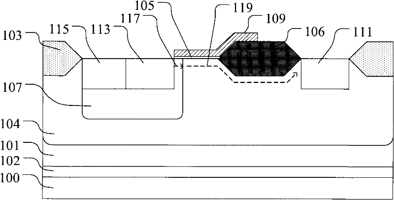
[0028] In the LDMOS transistor in the prior art, the field plate of the LDMOS transistor is formed by using the LOCOS oxide layer, and the unique bird's beak region of the LOCOS oxide layer can make the gate electrode gradually expand from a thinner gate dielectric layer to a thicker field plate. This gradual gate electrode structure can weaken the surface electric field near the gate electrode, which is beneficial to improve the breakdown voltage of the LDMOS transistor.

[0029] However, the bird's beak region of the LOCOS oxide layer will partially sag the silicon-silicon oxide interface downward, and change the direction of the current flow in the drift region, which makes the electric field lines in the channel region bend, and the curved electric field lines As a result, the electric field lines near the drain region are concentrated, and channel punch-through is prone to occur.

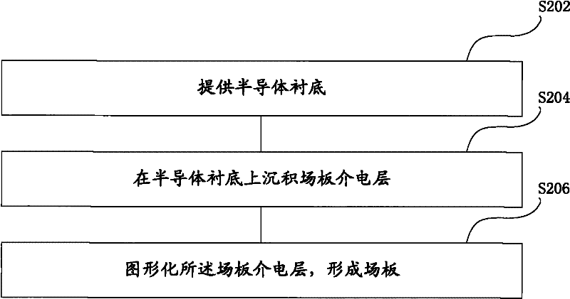
[0030] In view of the above problems, the inventor provides the following technical solutio...


PUM


Abstract

A method for manufacturing a laterally diffused metal oxide semiconductor transistor, comprising: providing a semiconductor substrate, depositing a field plate dielectric layer on the semiconductor substrate, patterning the field plate dielectric layer, and forming a laterally diffused metal oxide semiconductor transistor. Field plate of an oxide semiconductor transistor. The present invention makes field plates by depositing a field plate dielectric layer on a semiconductor substrate, and the electric field lines below the field plates do not bend, which solves the channel penetration problem caused by the bending of electric field lines; at the same time, through isotropic etching The method forms a slope-shaped transition at the edge of the field plate, and the slope-shaped transition at the edge of the field plate prevents the grid electrode on the field plate from being broken down due to tip discharge.

Description

technical field [0001] The invention relates to the technical field of semiconductors, and more specifically, the invention relates to a laterally diffused metal oxide semiconductor (LDMOS) transistor and a manufacturing method thereof. Background technique [0002] As a transistor compatible with the standard CMOS manufacturing process, LDMOS transistors are widely used in various high-voltage circuits and radio frequency circuits. Compared with ordinary MOS transistors, LDMOS transistors have a lightly doped drift region formed in the channel region between the source and drain, and the lightly doped drift region has higher resistance, and the uniform electric field in the drift region Carriers are maintained to pass at the saturation velocity. LDMOS transistors have a high breakdown voltage, therefore, LDMOS transistors are very suitable for high-voltage circuits. [0003] The Chinese patent application with application number 200710044405.5 discloses an LDMOS device an...

Claims


Application Information

Patent Timeline
Patent Type & Authority Applications(China)
IPC IPC(8): H01L21/336H01L29/78H01L29/06
Inventor 桂林春王乐林奕琼
Owner CSMC TECH FAB1
Why Eureka
Try Eureka