Check patentability & draft patents in minutes with Patsnap Eureka AI!

Polysilicon cleaning method and cleaning device, and polysilicon manufacturing method

A cleaning device and polysilicon technology are applied in the cleaning and cleaning device of polysilicon, and the manufacturing field of polysilicon, which can solve the problems of lowering the quality of monocrystalline silicon and achieve high-quality effects.

Active Publication Date: 2011-11-30
高纯度硅股份有限公司
View PDF8 Cites 5 Cited by
  • Summary
  • Abstract
  • Description
  • Claims
  • Application Information

AI Technical Summary

Problems solved by technology

If these pollutants or oxide films are mixed into the manufacturing process of single crystal silicon, the quality of single crystal silicon will be significantly reduced

Method used


Image

  • Polysilicon cleaning method and cleaning device, and polysilicon manufacturing method
  • Polysilicon cleaning method and cleaning device, and polysilicon manufacturing method
  • Polysilicon cleaning method and cleaning device, and polysilicon manufacturing method

Examples


Embodiment

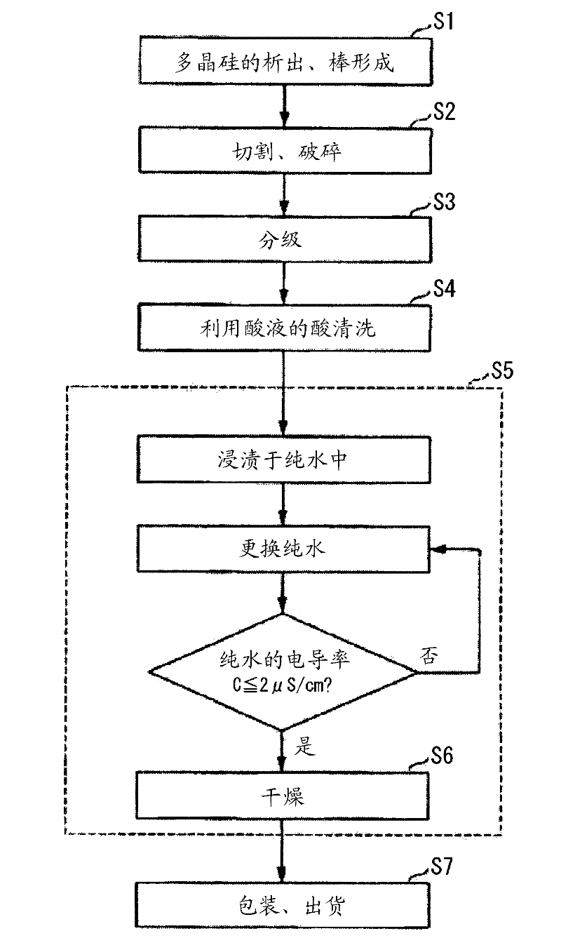
[0100] According to the above-mentioned cleaning method, polysilicon was cleaned several times under different conditions.

[0101] For any one cleaning, a large amount of one type of polysilicon is dipped in one washing tank. In Table 1, "thick block (large)" refers to a material with a large block of polysilicon, specifically, a material with a diameter of about 50 mm to 100 mm, and "thick block (small)" refers to a material with a small block of polysilicon , specifically, refers to a substance with a diameter of about 5 mm to 50 mm. Also, a plurality of baskets accommodating polycrystalline silicon lumps in an amount of 5 kg were prepared, and these were immersed in one water washing tank with a required weight according to each condition. The analysis of impurities was performed using ICP-MS (Inductively Coupled Plasma Mass Spectrometry). However, since the amount of impurities actually measured was extremely small, the lower limit of quantification is shown in Table 1....


PUM

PropertyMeasurementUnit
diameteraaaaaaaaaa
diameteraaaaaaaaaa
diameteraaaaaaaaaa

Abstract

A polycrystalline silicon cleaning method comprising a pickling step using an acid solution and a water washing step of washing with pure water after the pickling step, in which the polycrystalline silicon is immersed in a stored pure In the washing tank of water, replace the pure water in the washing tank at least once to remove the above-mentioned acid liquid remaining on the surface of the polysilicon, and measure the conductivity (C) of the pure water in the washing tank at the same time, according to the above-mentioned conductivity (C) measured value to judge the end of the above-mentioned washing process.

Description

technical field [0001] The present invention relates to a method of cleaning polysilicon used as a raw material of silicon for semiconductors, a polysilicon cleaning device suitable for carrying out the cleaning method, and a method of producing polysilicon using the cleaning method. [0002] This application claims the priority of Japanese Patent Application No. 2008-332320 filed on December 26, 2008, and the contents thereof are incorporated herein by reference. Background technique [0003] As a raw material of a silicon single crystal wafer for semiconductor use, for example, extremely high-purity polycrystalline silicon of 99.999999999% or higher is used. The polycrystalline silicon can be produced by a method called the Siemens method as follows: Trichlorosilane (SiHCl 3 ) gas and hydrogen to precipitate high-purity polysilicon on the silicon core rod. In this way, an ingot of approximately cylindrical polycrystalline silicon having a diameter of about 140 mm was obt...

Claims


Application Information

Patent Timeline
Patent Type & Authority Applications(China)
IPC IPC(8): C30B29/06B08B3/08
CPCC01B33/037C30B29/06C01B33/02C01B33/035B08B3/08
Inventor 堺一弘渥美彻弥宫田幸和
Owner 高纯度硅股份有限公司
Features
  • R&D
  • Intellectual Property
  • Life Sciences
  • Materials
  • Tech Scout
  • Unparalleled Data Quality
  • Higher Quality Content
  • 60% Fewer Hallucinations
Learn More