Substrate processing system and substrate processing method

A substrate processing system and processing scheme technology, applied in the directions of transportation and packaging, conveyor objects, electrical components, etc., can solve problems such as inability to perform exposure processing, poor equipment, and failure to solve problems.

Active Publication Date: 2011-12-07
TOKYO ELECTRON LTD
View PDF5 Cites 7 Cited by
  • Summary
  • Abstract
  • Description
  • Claims
  • Application Information

AI Technical Summary

Problems solved by technology

[0006] However, in the substrate processing system described above, when the wafer W1 coated with the resist by the coating device is carried into the exposure device through the carrier 1, the wafer W1 of the carrier 2 transported to the exposure device is carried out first in the exposure device. In the process of 102, there is a problem that the exposure process cannot be performed within a predetermined time after the coating of the wafer W1 due to maintenance or a sudden defect in the device.
In Patent Document 1, there is no description about such a problem, and the problem cannot be solved.

Method used


Image

  • Substrate processing system and substrate processing method
  • Substrate processing system and substrate processing method
  • Substrate processing system and substrate processing method

Examples


no. 1 approach

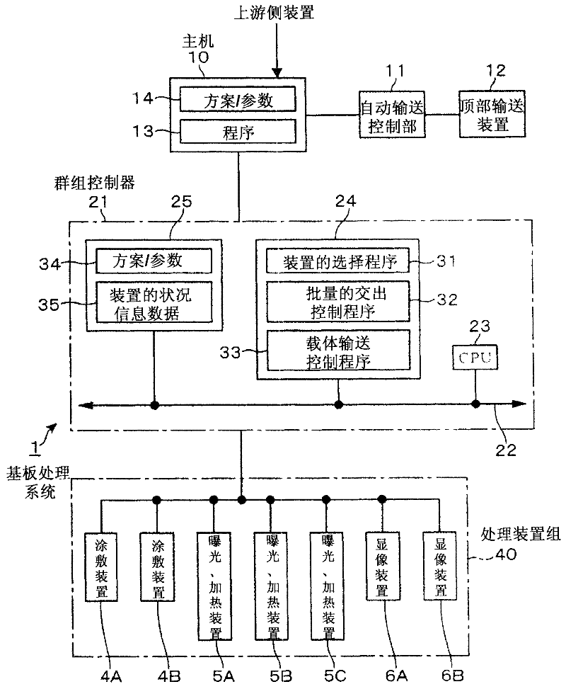
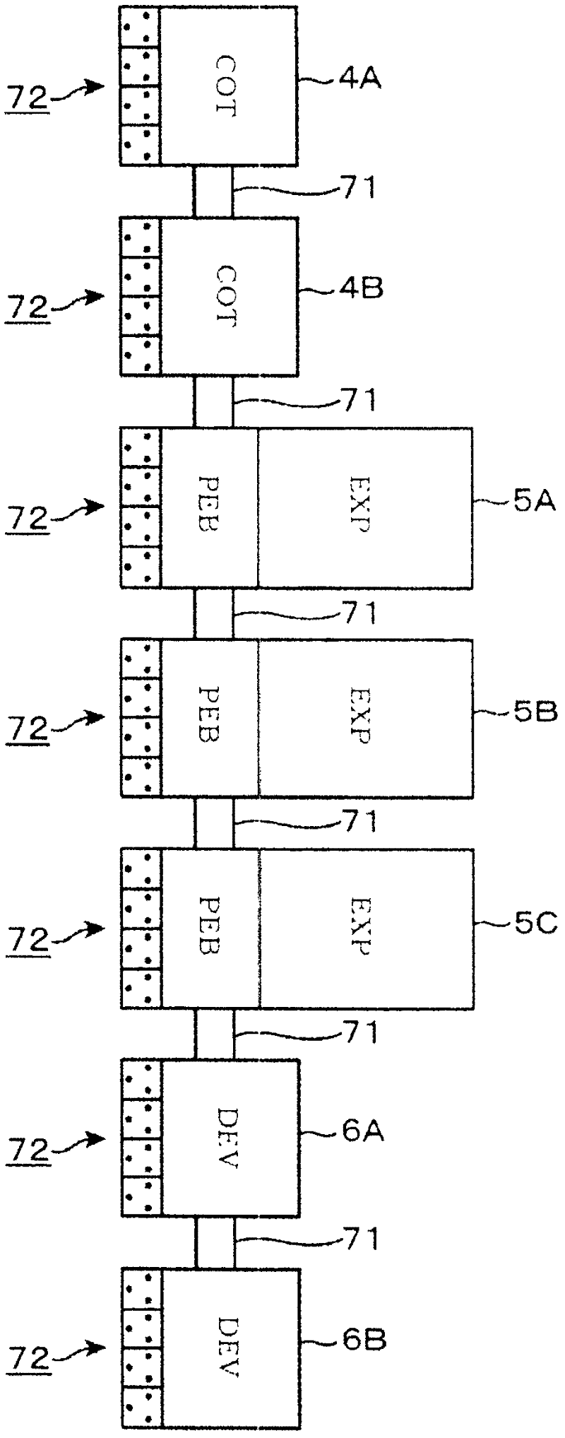
[0102] figure 1 It is an overall configuration diagram of a substrate processing system 1 as an embodiment of the present invention. The substrate processing system 1 is composed of a group of processing devices 40, and the carrier C is transported between the processing devices to form a resist pattern on the wafer W. A plurality of wafers W of the same type are accommodated in one carrier C, and the wafers W of the same type are called a lot. The substrate processing system 1 includes a host computer 10 , a group controller 21 , a top transport device 12 , and the processing device group 40 described above. The processing device group 40 includes: coating devices 4A, 4B; exposure and heating devices 5A to 5C; and developing devices 6A, 6B.

[0103] The main machine 10 is connected to the top conveying device 12 through the automatic conveying control unit 11 . In addition, the host computer 10 is connected to the group controller 21 and connected to the processing device ...

no. 2 approach

[0152] Figure 13 The layout of the substrate processing system 121 of the second embodiment is shown. The coating devices 4A, 4B, exposure devices 5A, 5B, developing devices 6A, 6B, and inspection devices 7A, 7B are connected in this order.

[0153] The inspection devices 7A and 7B include an inspection module for inspecting the surface state of the developed wafer W, and the inspection devices 7A and 7B are the same as the coating device 4A except that the above-mentioned inspection module is mounted on the processing station 101 instead of the coating module. to constitute. The developed wafer W is inspected by the inspection device 7A or 7B. The carrier C is conveyed from the coating device 4A side to the inspection device 7B side, and a common carry-out stack 79 is provided at the carrier station 72 of the inspection device 7B.

[0154] In this substrate processing system 121, similarly to the substrate processing system 1, maintenance information, the processing statu...


PUM


Abstract

Provided is a substrate processing system including a group controller which determines a combination of processing apparatuses having the shortest total processing time including the processing end time in a final processing apparatus, determines a predictable elapsed time up to a processing start time by a predetermined downstream processing apparatus for a wafer lot from a processing end time of the wafer lot by a predetermined processing apparatus in the combination of the processing apparatuses, and determines a timing of discharging the substrate to the predetermined processing apparatus or an upstream processing apparatus of the predetermined processing apparatus so that the predictable elapsed time is set within a predetermined time when the predictable elapsed time exceeds the predetermined time.

Description

technical field [0001] The present invention relates to a substrate processing system and a substrate transfer method for processing a substrate including a photolithography process. Background technique [0002] In the manufacturing process of a semiconductor device, a pattern should be formed on a semiconductor wafer (hereinafter referred to as "wafer"), and then a photolithography process should be performed. In the photolithography process, the following processes are performed, that is, a resist coating process of the wafer, an exposure process of exposing the wafer after the resist coating using an exposure mask, and a development process of performing a development process of the exposed wafer. like processing. [0003] The photolithography process in the semiconductor device manufacturing process is performed by a resist patterning system connected to an automatic carrier transport system in a factory. A lot consisting of a plurality of wafers of the same type is a...

Claims


Application Information

Patent Timeline
Patent Type & Authority Applications(China)
IPC IPC(8): H01L21/00H01L21/677
CPCH01L21/67778H01L21/67745H01L21/67276
Inventor 月野木涉山本雄一
Owner TOKYO ELECTRON LTD
Why Eureka
Try Eureka