A kind of led device without gold wire

An LED device, no gold wire technology, applied in the field of flip-chip light-emitting diode devices, can solve the problems of complex process, affecting production efficiency, production difficulty, etc., to achieve the effect of enhancing light-emitting effect, improving production efficiency, and improving reliability

Inactive Publication Date: 2011-12-07
APT ELECTRONICS
View PDF5 Cites 39 Cited by
  • Summary
  • Abstract
  • Description
  • Claims
  • Application Information

AI Technical Summary

Problems solved by technology

Although this structure solves the problem of the thermal quenching effect of phosphor, it needs to coat multiple layers of phosphor on the transparent adhesive layer, which makes the process more complicated and affects production efficiency. At the same time, the phosphor layer in this structure contains a reflection Layers also bring difficulty to production

Method used


Image

  • A kind of led device without gold wire
  • A kind of led device without gold wire
  • A kind of led device without gold wire

Examples


Embodiment 1

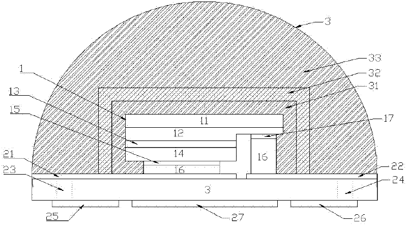
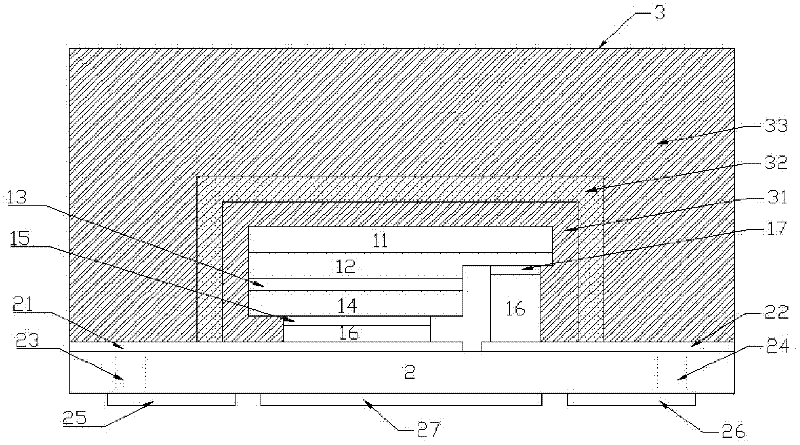
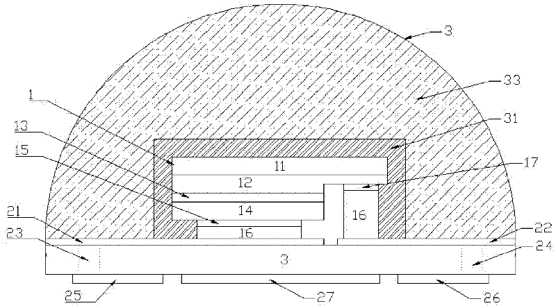
[0049] Such as figure 1 As shown, a gold-wire-free LED device includes an LED chip 1 , a substrate 2 and a packaging structure 3 . The LED chip 1 is flip-chip mounted on the substrate 2 , and the encapsulation structure 3 is disposed on the substrate 2 and surrounds the LED chip 1 .

[0050]The LED chip 1 includes a sapphire substrate 11 , an N-type GaN 12 , a light emitting layer 13 , a P-type GaN 14 , a P electrode 15 , a metal bump 16 and an N electrode 17 . N-type GaN 12 is grown on the sapphire substrate 11 , a light-emitting layer 13 is grown on the N-type GaN 12 , and a P-type GaN 14 is grown on the light-emitting layer 13 . Through process steps such as photolithography, etching, metal layer deposition and passivation layer protection, and finally through the split process, P electrodes 15 and metal bumps 16 are formed on the P-type GaN 14 layer, and on the N-type GaN 12 N electrodes 17 and metal bumps 16 are formed on the LED chip, and the P electrodes 15 and N elec...

Embodiment 2

[0065] The difference between embodiment 2 and embodiment 1 is that the shape of the optical structure layer 33 in the package structure 3 in embodiment 2 is a square structure. The optical structure layer 33 is used to adjust the external shape, and can meet different optical requirements of the packaging structure, and its material can be one or a combination of PC, PMMA, Silicone, EP, PET, and glass. The square shape structure can be made into a small volume and easy to shape.

Embodiment 3

[0067] The difference between embodiment 3 and embodiment 1 is that the optical structure layer 33 in the encapsulation structure 3 contains light conversion substances, and the light conversion substances are organic dyes, rare earth light-emitting organic complexes, YAG, LuAG, Silicate, (Ca , Sr)AlSiN 3 One or more mixtures, the light conversion substance and the optical structure layer material in liquid state are pre-mixed together, and then formed by coating, molding and other process steps. By mixing the light-converting substance into the optical structure layer 33, the functions of light conversion and designing the optical outer layer structure are realized at the same time, which greatly improves the production efficiency and reduces the production cost.

[0068] Compared with the prior art, the present invention flip-chips the LED chip 1 on the ceramic substrate 2, effectively improving the heat dissipation effect of the LED device. The first through hole 23 and th...


PUM


Abstract

The invention discloses a gold-wire-free LED device. The LED chip is flipped on a substrate, and the P pole and N pole of the LED chip are led to the second metal electrode layer on the lower surface of the substrate through a through hole on the substrate. A heat dissipation metal pad is provided on the lower surface to realize the purpose of separating thermoelectric channels of the LED device, and greatly enhance the heat dissipation performance and reliability of the LED device. At the same time, the present invention also has a multi-layer packaging structure, the light conversion material layer can be far away from the LED chip, effectively prevents the thermal quenching effect of the light conversion material, and greatly improves the uniformity of light color of the LED device.

Description

technical field [0001] The invention relates to a light-emitting diode device, in particular to a flip-chip light-emitting diode device. Background technique [0002] Light-emitting diode (LED) is an electroluminescent device processed by semiconductor manufacturing technology. The main principle of light emission is that the compound semiconductor material is loaded with a forward voltage, and the active electrons and holes recombine to generate photons. Eye recognition produces visible light. At present, because the brightness problem of LEDs has been greatly improved, LEDs are widely used in various fields, including backlight units, automobiles, electric signals, traffic lights, lighting devices, and the like. [0003] In order to make high-power LED lighting have higher brightness, the input current of LED can be increased. However, the increase of the current causes the LED chip to generate a lot of heat. In order to improve the reliability of the LED chip and preven...

Claims


Application Information

Patent Timeline
Patent Type & Authority Applications(China)
IPC IPC(8): H01L33/48H01L33/64H01L33/62H01L25/075
CPCH01L2224/14H01L2224/16225
Inventor 万垂铭陈海英周玉刚肖国伟
Owner APT ELECTRONICS
Why Eureka
Try Eureka