
Integrator circuit and δς modulator having the same

A technology of integrators and modulators, which is applied in the direction of incremental modulation, instruments, electrical components, etc., can solve the problems of limited gain frequency bandwidth of operational amplifiers and the influence of integrator circuit characteristics, etc., to suppress damped oscillations, improve SNR, and improve The effect of the characteristic

Inactive Publication Date: 2011-12-07
PANASONIC CORP
View PDF1 Cites 11 Cited by
  • Summary
  • Abstract
  • Description
  • Claims
  • Application Information

AI Technical Summary

Problems solved by technology

[0003] Here, the gain frequency bandwidth of the operational amplifier of the actual circuit is limited, and the characteristics of the integrator circuit are also affected by it

Method used


Image

  • Integrator circuit and δς modulator having the same
  • Integrator circuit and δς modulator having the same
  • Integrator circuit and δς modulator having the same

Examples


Embodiment Construction

[0027] Hereinafter, embodiments of the present invention will be described in detail with reference to the drawings.

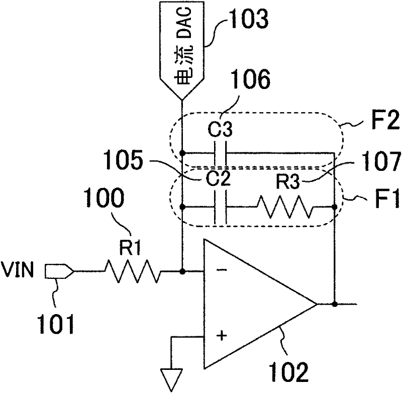
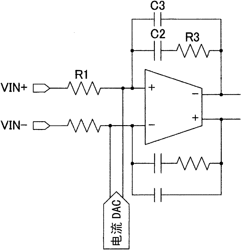
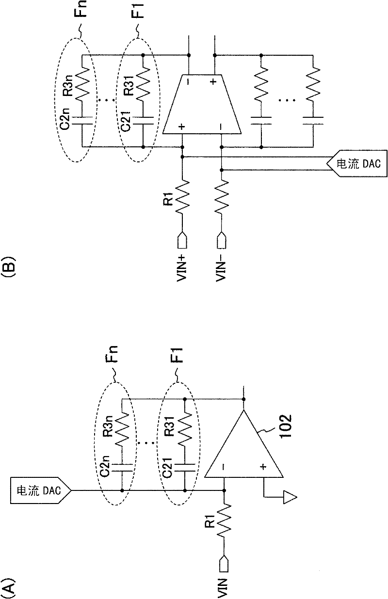
[0028] figure 1 It is a circuit diagram showing the structure of the integrator circuit of embodiment. exist figure 1 100 is an input resistor ( R1 ), 101 is a voltage input terminal, and 102 is an operational amplifier, and the voltage input terminal 101 is connected to the inverting input terminal of the operational amplifier 102 via the input resistor 100 . The output of the current source DA converter 103 is also connected to the inverting input terminal of the operational amplifier 102 . In addition, first and second feedback paths F1 and F2 are provided between the output terminal and the inverting input terminal of the operational amplifier 102 . In the first feedback path F1, the first integrating capacitive element 105 (C2) and the first resistive element 107 (R3) are provided in series. In the second feedback path F2, a second integrating capac...


PUM


Abstract

The purpose of providing an integrator circuit capable of alleviating disturbance of a current waveform of a current source DA converter is to improve the SNR of, for example, a ΔΣ modulator. An integrator circuit having an operational amplifier (102) with a feedback path (F1, F2) provided in parallel between an output terminal and an inverting input terminal of the operational amplifier (102). In the feedback path (F1), an integral capacitive element (105) and at least one resistive element (107) are arranged in series, and in the feedback path (F2), a second integral element having a capacitance smaller than the integral capacitive element (105) is provided. Capacitive element (106).

Description

technical field [0001] The present invention relates to an integrator circuit used in a loop filter or the like of a ΔΣ modulator. Background technique [0002] A continuous-time delta-sigma modulator has a loop filter. This loop filter is often constituted by an active type filter using an operational amplifier or the like. Figure 6 (A) is an example of an integrator circuit within a loop filter. [0003] Here, the gain bandwidth of the operational amplifier of the actual circuit is limited, and the characteristics of the integrator circuit are also affected by it. For this, in Figure 7 As shown by the solid line in , in terms of gain characteristics and phase characteristics, a second pole occurs on the high-frequency side of the frequency. [0004] As a method of correcting it, as disclosed in Non-Patent Document 1, there is known a Figure 6 The method shown in (B) is to insert a resistor in series with the integrating capacitor. Thus, if Figure 7 As shown in the...

Claims


Application Information

Patent Timeline
Patent Type & Authority Applications(China)
IPC IPC(8): H03M3/02H03M1/66H03M1/74H03M7/32
CPCH03M3/376H03M3/43H03M3/454
Inventor 松川和生道正志郎三谷阳介小畑幸嗣
Owner PANASONIC CORP
Learn More