Estimation method of the relative position of the radiation displacement damage area in the coms device in the channel

A displacement damage and irradiation technology, applied in the field of estimating the position of irradiation displacement damage, can solve the problems affecting the static and transient characteristics and reliability of CMOS devices, and achieve the effect of easy operation and simple method.

Active Publication Date: 2011-12-14
SEMICONDUCTOR MANUFACTURING INTERNATIONAL (BEIJING) CORP +1
View PDF3 Cites 4 Cited by
  • Summary
  • Abstract
  • Description
  • Claims
  • Application Information

AI Technical Summary

Problems solved by technology

However, the working mechanism of CMOS devices mainly depends on the conductive channel formed by the surface inversion layer. The damage caused by heavy ions in the channel region will seriously affect the static and transient characteristics of CMOS devices and cause

Method used


Image

  • Estimation method of the relative position of the radiation displacement damage area in the coms device in the channel
  • Estimation method of the relative position of the radiation displacement damage area in the coms device in the channel
  • Estimation method of the relative position of the radiation displacement damage area in the coms device in the channel

Examples


Embodiment Construction

[0028] The present invention is further illustrated below by means of examples, but the present invention is not limited to the scope of the examples.

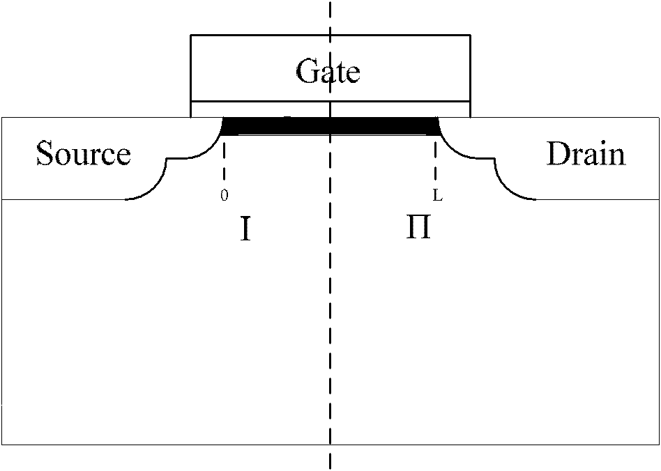
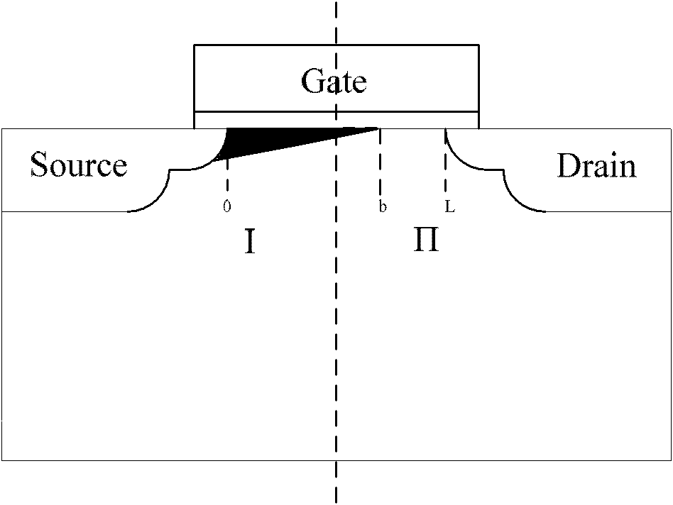
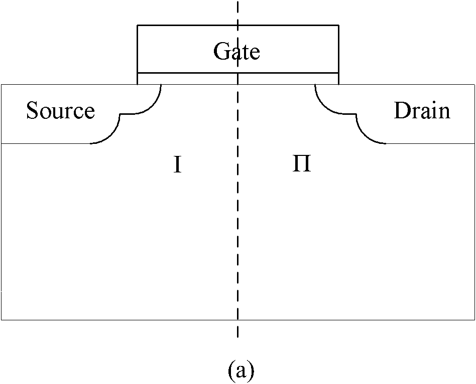
[0029] The intrinsic capacitance of a CMOS device is the capacitance from the gate to the channel. Its size and its division in the gate-source capacitance Cgs, gate-drain capacitance Cgd, and gate-to-body capacitance Cgb depend on the working area and port voltage. When the CMOS device is in the cut-off region, there is no channel under the gate, and the gate-source capacitance and gate-drain capacitance are 0; when the device is in the strong inversion region, the gate and the body are shielded by the channel, and the gate-body Capacitance is negligible. The gate-source capacitance or the gate-drain capacitance can be understood as the change of the gate electrode charge caused by the potential change of the source terminal or the drain terminal relative to the gate terminal potential, and the size of the gate-source capacit...


PUM


Abstract

The invention discloses a method for estimating relative position of a radiation displacement damage area of a COMS (Complementary Metal Oxide Semiconductor) device in a channel. In the method, the groove of the CMOS device is partitioned into two parts; a part close to a source end is an area I; and a part to a drain end is an area II. When the situation after radiation is compared with the situation before radiation, the radiation displacement damage area is in the area I if the gate source capacitance is decreased while the gate drain capacitance is increased; and the radiation displacement damage area is in the area II if the gate source capacitance is increased while the gate drain capacitance is decreased. Specific to the CMOS device, relative position of the radiation displacement damage area in the groove is represented according to the change of intrinsic capacitance before and after radiation. The method is simple, is easy to operate, and plays a great role in researching single particles, modeling single particles and reinforcing integrated circuits; and a thought for determining the position of the radiation displacement damage area on the CMOS device is provided.

Description

technical field [0001] The invention relates to a method for estimating the position of radiation displacement damage, in particular to a method for estimating the relative position of the radiation displacement damage area of ​​a CMOS device in a channel. Background technique [0002] With the wide application of integrated circuit technology in the field of aerospace, the irradiation effect of a large number of cosmic rays in the universe and outer space on integrated circuits will cause the degradation of electronic components and circuit characteristics. Radiation effect has become the main cause of failure of space components. It is of great significance to study the radiation effect of deep submicron integrated circuits working in space environment and nuclear explosion irradiation environment, and to develop anti-irradiation integrated circuits. [0003] The interaction between high-energy particles and semiconductor materials will cause displacement damage in semico...

Claims


Application Information

Patent Timeline
IPC IPC(8): G01B7/00
Inventor 黄如谭斐安霞张兴
Owner SEMICONDUCTOR MANUFACTURING INTERNATIONAL (BEIJING) CORP
Why Eureka
Try Eureka