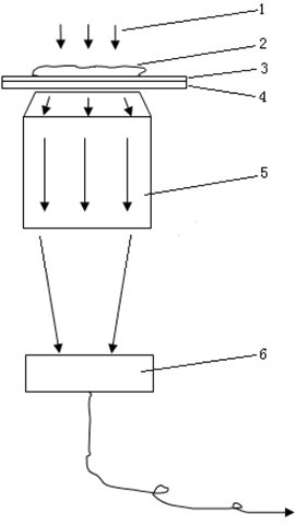
Sub-pixel segmentation coding microscopy imaging device
An imaging device and coding technology, used in measurement devices, scanning probe microscopy, instruments, etc., can solve the problem that the resolution of the microscope cannot continue to improve the resolution and field of view, the control is difficult, and the imaging speed of the near-field optical microscope is slow. And other issues
- Summary
- Abstract
- Description
- Claims
- Application Information
AI Technical Summary
Problems solved by technology
Method used
Image

Examples
Embodiment 1
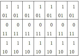
[0148] Embodiment 1, M=3, N=5, the sub-arrays constituting the sub-wavelength pinhole array are 3rd order, and the number of columns necessary for encoding is P=2;
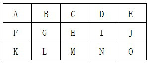
[0149] Such as figure 2 As shown, the image obtained by the area array photodetector is composed of 3×5 pixels, and each pixel is represented by the letters A~O; the sub-wavelength pinhole array is composed of 3×5 sub-arrays and 2 columns of small holes necessary for coding. Each sub-array is composed of holes, and each sub-array is composed of any row of a 3-row and 3-column cyclic s matrix composed of 0 and 1; the first row is 101,
[0150] When forming a subwavelength pinhole array, it is an array of 3 rows and 17 columns:
[0151] 10110110110110110
[0152] 10110110110110110
[0153] 10110110110110110,
[0154] or:
[0155] 01101101101101101
[0156] 01101101101101101
[0157] 01101101101101101,
[0158] or:
[0159] 11011011011011011
[0160] 11011011011011011
[0161] 11011011011011011,
[0162]...
Embodiment 2
[0165] Embodiment 2, M=3, N=5, the sub-arrays that make up the sub-wavelength pinhole array are 15 orders, and the number of additional columns necessary for encoding is P-1=14; each sub-array is composed of the same, all are composed of 0 and 1 Any row of the formed 15-row and 15-column cyclic s-matrix, the first row is 000100110101111; to simplify the expression, the following character correspondences: Octal 0, 1, 2, 3, 4, 5, 6, 7 respectively represent binary 000, 001 , 010, 011, 100, 101, 110, 111, the first line is 04657;
[0166] The subwavelength pinhole array is composed of 3 rows and 89 columns:
[0167] 04657046570465704657046570465+11
[0168] 04657046570465704657046570465+11
[0169] 04657046570465704657046570465+11;
[0170] In the above array, the two rightmost columns are in binary representation, and the remaining columns are in octal representation.
Embodiment 3
[0171] Embodiment 3, M=3, N=5, the sub-arrays forming the sub-wavelength pinhole array are 15 orders, and the number of additional columns necessary for encoding is 14;
[0172] Each sub-array is a 5×3 array, and the first row 000100110101111 of the 15-row and 15-column circular s-matrix composed of 0 and 1 is formed by folding 5 rows, and the folding method of 5 rows and 3 columns is:
[0173] 000
[0174] 100
[0175] 110
[0176] 101
[0177] 111
[0178] The first 5 rows of the corresponding subwavelength pinhole array are made as follows:
[0179] 00010011010111100010011010111
[0180] 10011010111100010011010111100
[0181] 11010111100010011010111100010
[0182] 10111100010011010111100010011
[0183]11100010011010111100010011010
[0184] Among them, the first 5 rows of the subwavelength pinhole array are constructed in the following way, from left to right:
[0185] 1st subarray, 2nd subarray, ... 3rd subarray, 5×14 additional subarrays,
[0186] In the 2nd to ...
PUM
 Abstract
Description
Claims
Application Information
 - R&D
- Intellectual Property
- Life Sciences
- Materials
- Tech Scout
- Unparalleled Data Quality
- Higher Quality Content
- 60% Fewer Hallucinations
Browse by: Latest US Patents, China's latest patents, Technical Efficacy Thesaurus, Application Domain, Technology Topic, Popular Technical Reports.
© 2025 PatSnap. All rights reserved.Legal|Privacy policy|Modern Slavery Act Transparency Statement|Sitemap|About US| Contact US: help@patsnap.com