

Integrated structure and manufacturing method of an infrared focal plane array detector
An array detector, infrared focal plane technology, applied in the direction of electric radiation detectors, semiconductor devices, radiation control devices, etc., can solve the problems of signal processing integrated circuit IC stability, unfavorable reliability, temperature rise, heat accumulation, etc. , to achieve the effect of reducing thermal interference and improving stability
- Summary
- Abstract
- Description
- Claims
- Application Information
AI Technical Summary
Problems solved by technology
Method used
Image

Examples
Embodiment 1
[0044] Embodiment one (flow process is as figure 2 shown)
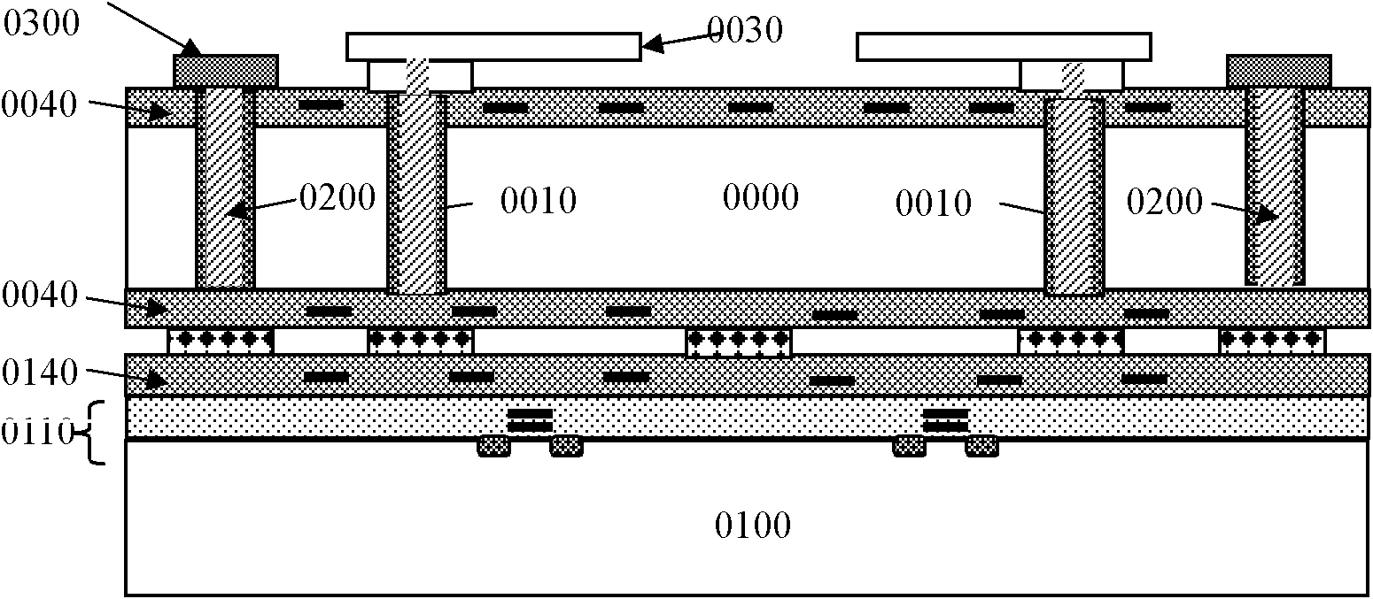
[0045] Step 1, such as Figure 2(a) ~ Figure 2(d)As shown, a first wafer is provided, a first through-silicon via micro-interconnection TSV and a second through-silicon via micro-interconnection TSV are provided on the first wafer, and a first through-silicon via micro-interconnection TSV is fabricated on the first surface of the first wafer. An electrical contact element, the first TSV micro-interconnection TSV and the second TSV micro-interconnection TSV are electrically connected to the first electrical contact element. First, photolithography, making the photolithography mask of the first through-silicon via micro-interconnection TSV and the second through-silicon via micro-interconnection TSV, deep reactive ion etching (DRIE) silicon substrate, making the first TSV 0011 and the second TSV 0210, such as figure 2 (a) shown. The first TSV 0011 and the second TSV 0210 can also be fabricated using other techniqu...
Embodiment 2
[0050] Embodiment two (flow process is as image 3 shown)
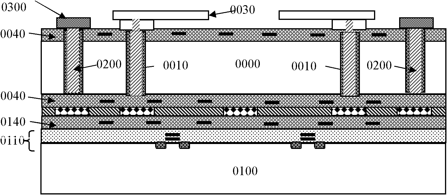
[0051] Step 1, such as Figure 3(a) ~ Figure 3(d) As shown, a first wafer is provided, and the first TSV and the second TSV are fabricated on the first wafer. On the first wafer, the Fabricating a first electrical contact element on one surface, the first through-silicon via micro-interconnection TSV and the second through-silicon via micro-interconnection TSV are electrically connected to the first electrical contact element; on the first wafer A patterned adhesive layer 0050 is formed on the first surface, exposing the electrical contact element 0020; the outer surface of the first electrical contact element 0020 is at the same level as the outer surface 0050 of the patterned adhesive layer. First, photolithography, making the photolithography mask of the first through-silicon via micro-interconnection TSV and the second through-silicon via micro-interconnection TSV, deep reactive ion etching (DRIE) silicon substr...
Embodiment 3
[0056] Embodiment three (flow process such as Figure 4 shown)
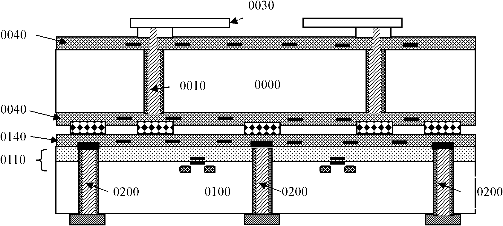
[0057] Step 1, such as Figure 4(a) ~ Figure 4(d) As shown, a first wafer is provided, and a first through-silicon via micro-interconnection TSV 0010 is provided on the first wafer to make a first electrical contact element 0020 on the first surface of the first wafer, and the first silicon A through-hole micro-interconnection TSV is electrically connected to the first electrical contact element. First, photolithography, making the photolithography mask of the first through-silicon via micro-interconnection TSV, deep reactive ion etching (DRIE) silicon substrate, making the first through-silicon hole 0011, as Figure 4 (a) shown. The first TSV 0011 can also be fabricated using other techniques, such as laser drilling. Electroplating fills the first through-silicon via from bottom to top. First, deposit a dielectric layer, a barrier layer, and an electroplating seed layer. The dielectric layer realizes the ele...
PUM
 Abstract
Description
Claims
Application Information