
Crystal silicon cell back field back pole and printing technology thereof

A technology of crystalline silicon battery and back field, applied in circuits, electrical components, sustainable manufacturing/processing, etc., can solve the problems of inability to passivate, block aluminum paste coverage, gettering, etc., and increase the passivation area , improve battery electrical performance, reduce the effect of recombination

Active Publication Date: 2013-08-21
微山县顺扬贸易有限公司
View PDF4 Cites 0 Cited by
  • Summary
  • Abstract
  • Description
  • Claims
  • Application Information

AI Technical Summary

Problems solved by technology

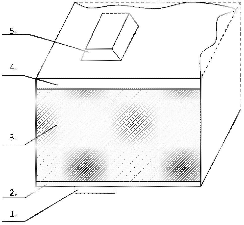
[0003] If the production is carried out according to the conventional battery production process, the back electrode is printed first and then the back field is printed, the area where the back electrode is located will block the coverage of the aluminum paste, that is, the area covered by the back electrode cannot form an aluminum back field, so it cannot play a passivation role. backside, gettering, etc., which is not conducive to the improvement of battery electrical performance

Method used


Image

  • Crystal silicon cell back field back pole and printing technology thereof
  • Crystal silicon cell back field back pole and printing technology thereof
  • Crystal silicon cell back field back pole and printing technology thereof

Examples


Embodiment 1

[0021] After the monocrystalline silicon wafer is diffused and coated on the light-receiving surface, the existing screen printing technology is used to print aluminum paste on its back surface. The aluminum paste is produced by Ruxing Company. The thickness of the printed aluminum paste is 30μm. After drying the aluminum paste at about 150°C, a continuous back electrode silver-aluminum paste is printed on the surface of the aluminum paste. The model of the back-electrode silver-aluminum paste is Flow 33462. The back electrode has a width of 2mm and a thickness of 15μm. Finally, follow-up production processes such as printing and sintering are carried out.

Embodiment 2

[0023] After the polycrystalline silicon wafer is diffused and coated on the light-receiving surface, the aluminum paste is printed on the back surface of the polysilicon wafer by screen printing technology. The aluminum paste is produced by Ruxing Company. The thickness of the printed aluminum paste is 40μm. After drying the aluminum paste at 200°C, a segmented back electrode silver paste is printed on its surface. The back electrode silver paste model is DuPont PV505, and the back electrode has a single width of 3mm and a thickness of 30μm. Finally, follow-up production processes such as printing and sintering are carried out.


PUM

PropertyMeasurementUnit
thicknessaaaaaaaaaa
thicknessaaaaaaaaaa
thicknessaaaaaaaaaa

Abstract

The invention relates to a crystal silicon cell back field back pole and a printing technology thereof. Aluminium paste is printed on the back surface of a crystal silicon sheet and is dried at certain temperature to form an aluminium back field; and back electrode slurry is printed on the dried aluminium paste surface to form a back electrode pattern. According to the printing technology, the area of the crystal silicon cell aluminium back field can be increased, crystal silicon back surface compound is reduced, and the gettering effect of the aluminium back field is increased, and the electric performance of the crystal silicon cell is effectively improved.

Description

Technical field: [0001] The invention relates to a crystalline silicon battery and its processing technology. Background technique: [0002] The conventional industrial screen printing process for crystalline silicon cells generally involves printing the back electrode first and then printing the aluminum back field. The aluminum back field can cover the exposed silicon wafer, passivate and protect the back surface of the crystalline silicon, and getter and separate the metal ion impurities in the silicon matrix. In addition, the aluminum back field also functions to collect current, conduct electricity, and converge the current to the back electrode. The main function of the back electrode is to draw current, which is used to contact the probe of the tester during testing, and to provide a welding base during welding. [0003] If the battery is produced according to the conventional battery production process, and the back electrode is printed first and then the back field is pr...

Claims


Application Information

Patent Timeline
Patent Type & Authority Patents(China)
IPC IPC(8): H01L31/18H01L31/0224
CPCY02P70/50
Inventor 杨雷何晨旭殷海亭钱金梁王冬松王步峰
Owner 微山县顺扬贸易有限公司
Learn More