
Manufacturing process for conductive carrying belt of electronic element

An electronic component and manufacturing process technology, applied in the manufacturing process field of electronic component carrier tape, can solve the problems of low product quality and high production cost

Active Publication Date: 2014-05-07
ZHEJIANG JIEMEI ELECTRONICS & TECH
View PDF12 Cites 0 Cited by
  • Summary
  • Abstract
  • Description
  • Claims
  • Application Information

AI Technical Summary

Problems solved by technology

[0005] The purpose of the present invention is to solve the problems of high production cost and low product quality caused by the two-stage process used in the production of the existing electronic component carrier tape, and discloses an integrated and continuous production with good tensile strength. Manufacturing process of conductive electronic component carrier tape with carrier tape pockets with high use and heat distortion temperature

Method used


Image

  • Manufacturing process for conductive carrying belt of electronic element
  • Manufacturing process for conductive carrying belt of electronic element
  • Manufacturing process for conductive carrying belt of electronic element

Examples


Embodiment 1

[0019] A manufacturing process of a carrier tape for conductive electronic components, comprising the following steps in turn: (1) making a polymer raw material into a thin film fluid, and processing the film fluid into an intermediate product of the carrier tape with pockets through a convex-concave mold, the polymerization The raw material of the product is a mixture of general-purpose polystyrene and conductive carbon black. According to the mass ratio, general-purpose polystyrene is 70% and conductive carbon black is 30%. The intermediate product of the carrier tape is punched and trimmed to obtain the finished product of the carrier tape for conductive electronic components.

[0020]In the above step (1), the polymer raw material is made into a film fluid through an extruder, and the convex and concave molds move in the same direction as the film exiting direction of the extruder and the moving speed is the same as the film exiting speed of the extruder, and the convex and...

Embodiment 2

[0027] A manufacturing process of a conductive electronic component carrier tape, the process steps are the same as in Example 1, the difference is that the proportions of general-purpose polystyrene and conductive carbon black in the polymer raw materials are different, and according to the mass ratio, the general-purpose polystyrene 80% styrene, 20% conductive carbon black, and the temperature of the convex and concave molds for film processing is controlled at about 220°C. The flow velocity of the film fluid is 18 m / min, and the downward movement speed of the convex-concave mold is consistent with the flow velocity of the film.

Embodiment 3

[0029] A manufacturing process of a conductive electronic component carrier tape, the process steps are the same as in Example 1, the only difference is that the proportion of general-purpose polystyrene and conductive carbon black in the polymer raw materials is different, and the general-purpose polystyrene is different in terms of mass ratio. Polystyrene is 90%, conductive carbon black is 10%, and the temperature of the convex and concave molds for film processing is controlled at about 225°C. The flow velocity of the film fluid is 22 m / min, and the downward movement speed of the convex-concave mold is consistent with the flow velocity of the film.

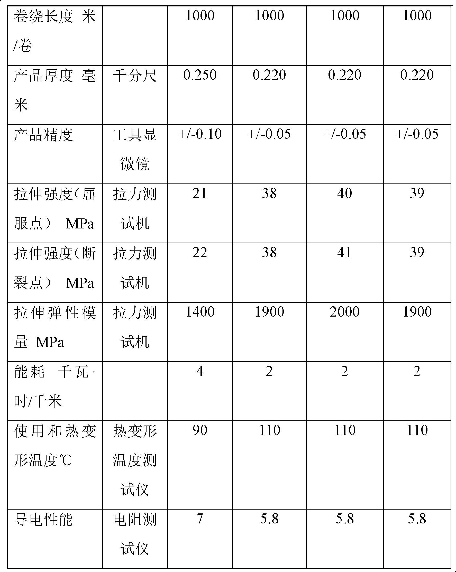
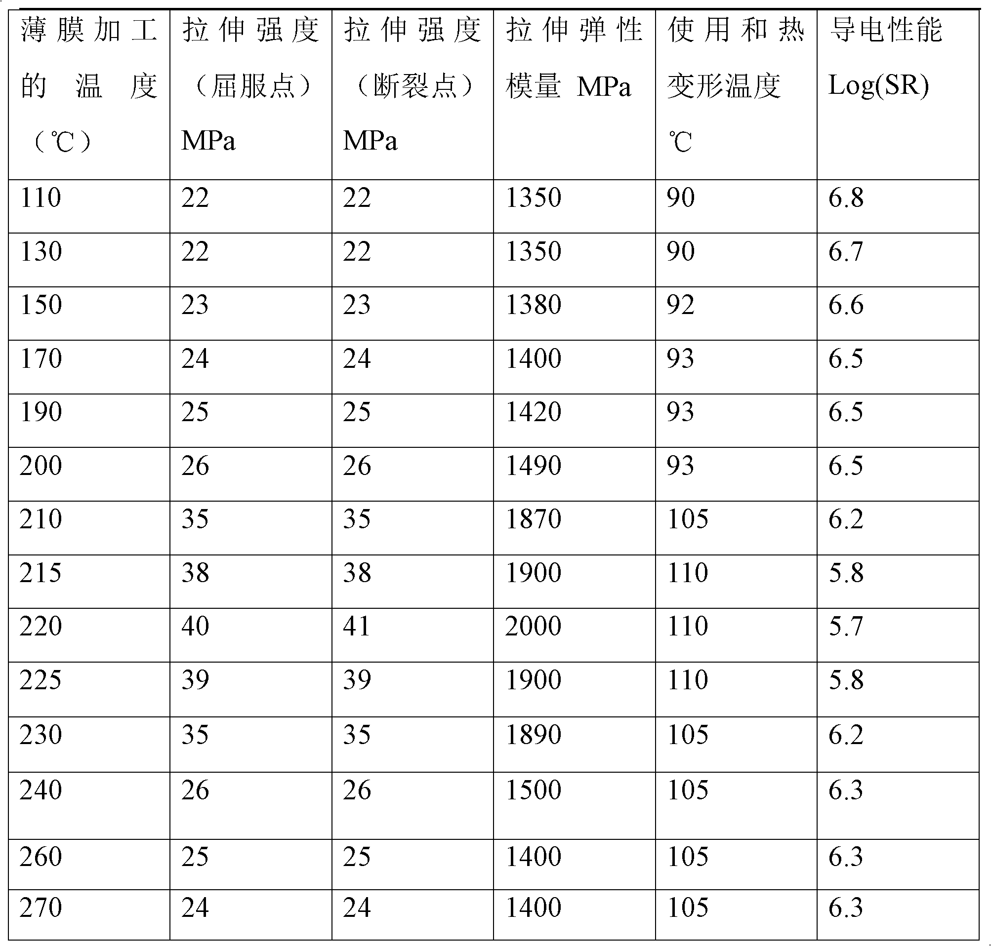
[0030] Following table is the data comparison of traditional product and 3 embodiments of this patent.

[0031]

[0032]

[0033] The above three embodiments are only preferred implementation modes of the present invention. Compared with the traditional two-stage process and intermittent equipment to produce electronic co...


PUM


Abstract

Disclosed is a manufacturing process for a carrying belt of an electronic element. A manufacturing process for a conductive carrying belt of the electronic element comprises the following steps in turn: (1) making a polymer raw material into a film fluid and adopting a convex-concave mould to process the film fluid into a intermediate product of the carrying belt with a pocket, wherein the polymer raw material is the mixture of 70-90% of general polystyrene and 10-30% of graphitized carbon black by mass percent; and the temperature for processing the film fluid with the convex-concave mould is controlled within a temperature range of 210 DEG C to 230 DEG C, and (2) punching and trimming the intermediate product of the carrying belt, thereby acquiring an end product of the conductive carrying belt of the electronic element. The manufacturing process for the conductive carrying belt of the electronic element has the advantages that the energy consumption of production is low, the length and the thickness both can be adjusted randomly, the production efficiency and the product quality are high, the conductivity is excellent, especially, the tensile strength is high, and the use temperature and the heat deformation temperature are greatly promoted.

Description

technical field [0001] The invention relates to a manufacturing process of an electronic component carrier tape, in particular to a manufacturing process of a conductive electronic component carrier tape. Background technique [0002] In the entire electronic product industry chain, the production of electronic component packaging and transportation carrier belts occupies a very important link. Electronic component packaging and transport carrier tape not only provides a medium for loading and transporting semiconductor integrated circuit electronic components, but more importantly, it is an important material that is essential for the subsequent high-speed, automated surface mount. With the invention and development of surface mount technology, the packaging form of semiconductor integrated circuits has gradually changed from the traditional pin type to the surface mount type, and the carrier tape of semiconductor electronic components has also emerged as the times require,...

Claims


Application Information

Patent Timeline
Patent Type & Authority Patents(China)
IPC IPC(8): B29D29/00B29C47/14B29C51/18B29C48/305
CPCB29C47/0054B29C47/92B29C47/0004B29C51/02B29K2995/0005B29C51/082B29C2947/92704B29C47/004B29C47/0021B29C48/0011B29C48/0017B29C48/022B29C48/08B29C48/92B29C2948/92704
Inventor 张澎涛
Owner ZHEJIANG JIEMEI ELECTRONICS & TECH
Learn More