Turnover type sampling hold circuit

A sample-and-hold circuit and flip-type technology, applied in the direction of logic circuit connection/interface layout, logic circuit coupling/interface using field effect transistors, physical parameter compensation/prevention, etc., can solve the problem of limiting input signal bandwidth, large distortion, Large consumption and other issues, to achieve the effect of increased input bandwidth, reduced nonlinearity, and reduced power consumption

Active Publication Date: 2013-09-04
CHENGDU SINO MICROELECTRONICS TECH CO LTD
View PDF2 Cites 0 Cited by
  • Summary
  • Abstract
  • Description
  • Claims
  • Application Information

AI Technical Summary

Problems solved by technology

[0003] In the traditional inverted sample-and-hold circuit, the input sampling switch S1 will introduce a large distortion due to the nonlinearity of its equivalent resistance and the body effect, which will greatly limit the bandwidth of the input signal
So the input frequency is limited within 100MHz
In addition, due to the closed-loop structure in the form of capacitors, the amplifier needs to have high bandwidth and gain to meet the requirements of high speed and high precision, which inevitably requires it to consume a lot of power to achieve a small settling time

Method used


Image

  • Turnover type sampling hold circuit
  • Turnover type sampling hold circuit
  • Turnover type sampling hold circuit

Examples


Embodiment Construction

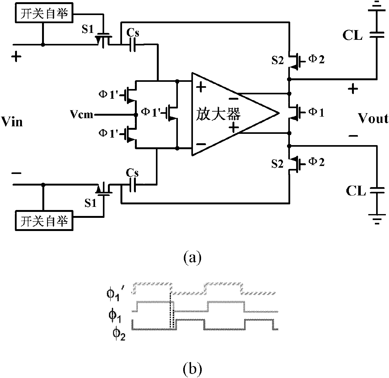
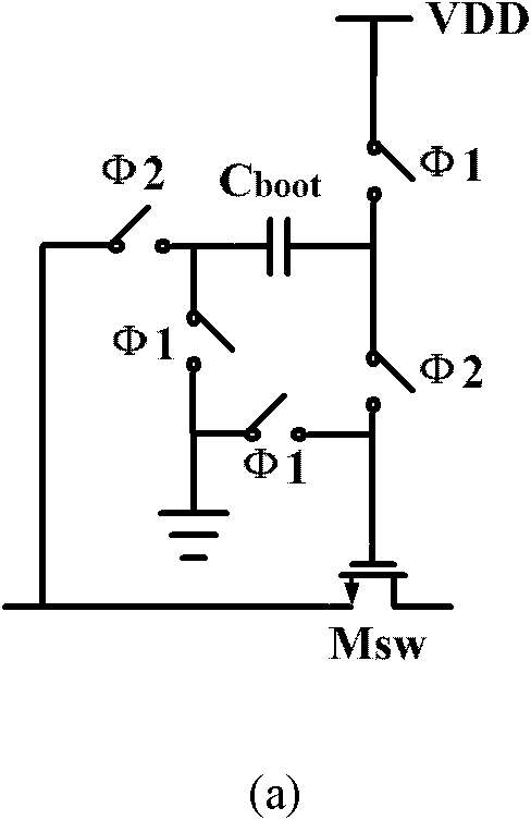
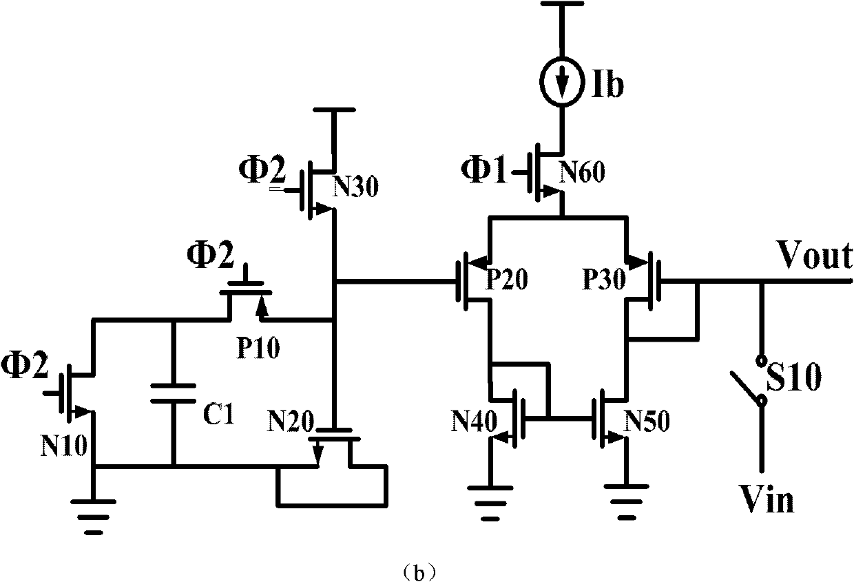
[0018] see Figure 2-4 .

[0019] The inverted sample-and-hold circuit of the present invention includes a first switch bootstrap circuit 101, a first sampling switch tube S11, a second switch bootstrap circuit 102, a second sampling switch tube S12, an amplifier and a first load capacitance circuit, a second The load capacitor circuit is characterized in that the first switch bootstrap circuit and the second switch bootstrap circuit have the same structure, the first switch bootstrap circuit 101 includes a charge compensation circuit, and the charge compensation circuit includes a first capacitor forming a loop C1 and the second NMOS transistor N20.

[0020] The first switch bootstrap circuit includes:

[0021] The gate of the first NMOS transistor N10 is connected to the second control signal Ф2, the drain is connected to the drain of the first PMOS transistor P10, and the source is grounded;

[0022] The gate of the first PMOS transistor P10 is connected to the second co...


PUM


Abstract

The invention discloses a turnover type sampling hold circuit, which relates to an integrated circuit technology. The circuit comprises a first switch bootstrap circuit, a first sampling switch tube, a second switch bootstrap circuit, a second sampling switch tube, an amplifier and a first load capacitive circuit and a second load capacitive circuit, and is characterized in that: the first switchbootstrap circuit and the second switch bootstrap circuit have the same structure; the first switch bootstrap circuit comprises a charge compensation circuit; and the charge compensation circuit comprises a first capacitor and a second NMOS (N-channel Metal Oxide Semiconductor) transistor which form a loop. Through the circuit, the nonlinearity introduced by a sampling switch is greatly reduced, input bandwidth is improved, meanwhile, the power consumption of the entire sampling hold circuit is reduced.

Description

technical field [0001] The present invention relates to integrated circuit technology. Background technique [0002] The flip-type sample-and-hold circuit of the prior art such as figure 1 as shown in (a), figure 1 (b) Control the clock for it. Its working process is as follows: In the sampling phase, that is, when Ф1 is high level and Ф2 is low level, the switch S1 is closed, the input signal is sampled to the capacitor CS, and the input terminal of the sample-and-hold amplifier is shorted to Vcm as a virtual ground. The output is also shorted. In the holding phase, switch S1 is turned off, S2 is closed, Ф1' jumps to low level earlier than Ф1, forming bottom plate sampling to reduce switch feedthrough, the amplifier is connected in a closed loop form, and the signal collected on CS before The load capacitance CL builds up. This completes the discrete sampling of the continuous signal. This circuit is suitable for high speed and high precision A / D converter. [0003] ...

Claims


Application Information

Patent Timeline
Patent Type & Authority Patents(China)
IPC IPC(8): H03M1/06H03K19/0185
Inventor 蔡化岑远军朱志勇张克林
Owner CHENGDU SINO MICROELECTRONICS TECH CO LTD
Why Eureka
Try Eureka