Method for manufacturing printed circuit board

A technology for printed circuit boards and manufacturing methods, which is applied to the secondary treatment of printed circuits, coating of non-metallic protective layers, etc., can solve problems such as inconsistent dimensional stability, high cost of coating process, and uneven ink thickness, and achieve Abandoning UV light exposure equipment, avoiding quality problems, and simplifying the process

Active Publication Date: 2013-05-22
SHENNAN CIRCUITS
View PDF3 Cites 0 Cited by
  • Summary
  • Abstract
  • Description
  • Claims
  • Application Information

AI Technical Summary

Problems solved by technology

[0002] The coating process on the surface of printed circuit boards has always been a process with high scrap rate and poor process stability. At present, silk screen printing or electrostatic spraying of green oil and black oil are mainly used to coat the surface insulating layer. During the coating process, it is necessary to Use expensive screen printing or electrostatic spraying equipment
[0003] The above-mentioned coating process of printed circuit boards has the following disadvantages: the thickness of the sprayed ink is not uniform during the spraying process, and it is easy to cause thin ink or ink accumulation defects; expensive silk screen or electrostatic spraying is required during the entire spraying process The cost of equipment and coating process is relatively high
In order to remove the excess solder resist layer, the photopolymer is exposed to the negative film after photopainting, and the excess solder resist layer is removed with an alkaline solution, and the printed circuit board expands with heat and contracts with cold during the multi-process processing. Physical properties determine that its dimensional stability is inconsistent, and there is a large precision error between the film and the object to be exposed

Method used


Image

  • Method for manufacturing printed circuit board
  • Method for manufacturing printed circuit board
  • Method for manufacturing printed circuit board

Examples


Embodiment Construction

[0036] The following will clearly and completely describe the technical solutions in the embodiments of the present invention with reference to the accompanying drawings in the embodiments of the present invention. Obviously, the described embodiments are only some, not all, embodiments of the present invention. Based on the embodiments of the present invention, all other embodiments obtained by persons of ordinary skill in the art without making creative efforts belong to the protection scope of the present invention.

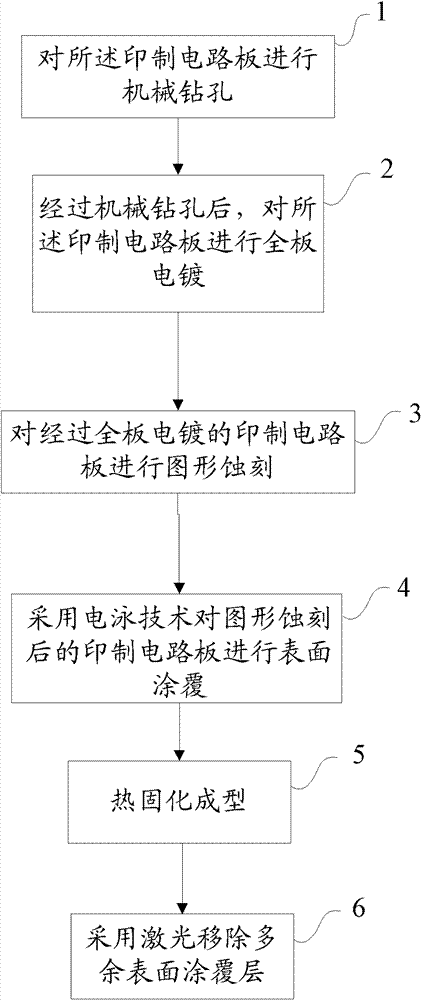
[0037] The embodiment of the invention discloses a method for manufacturing a printed circuit board, which improves the uniformity of coating on the surface of the circuit board and reduces the manufacturing cost of the entire circuit board.

[0038] Please refer to the attached figure 1 , figure 1 It is a schematic flowchart of a method for manufacturing a printed circuit board provided by an embodiment of the present invention.

[0039] The printed circuit...


PUM


Abstract

The embodiment of the invention discloses a method for manufacturing a printed circuit board. The method comprises the following steps of: 1), mechanically drilling the printed circuit board; 2), after mechanically drilling, electroplating the whole printed circuit board; 3), performing pattern etching on the electroplated whole printed circuit board; 4), performing surface coating on the printedcircuit board subjected to pattern etching by using an electrophoretic technique; 5), performing thermocuring molding; and 6), removing the unnecessary surface coating by using laser. By the method for manufacturing the printed circuit board, the uniformity of the surface coating of the printed circuit board is enhanced and the processing cost of the whole printed circuit board is reduced.

Description

technical field [0001] The invention relates to the technical field of PCB product processing, and more specifically, relates to a method for manufacturing a printed circuit board. Background technique [0002] The coating process on the surface of printed circuit boards has always been a process with high scrap rate and poor process stability. At present, silk screen printing or electrostatic spraying of green oil and black oil are mainly used to coat the surface insulating layer. During the coating process, it is necessary to Use expensive screen printing or electrostatic spraying equipment. [0003] The above-mentioned coating process of printed circuit boards has the following disadvantages: the thickness of the sprayed ink is not uniform during the spraying process, and it is easy to cause thin ink or ink accumulation defects; expensive silk screen or electrostatic spraying is required during the entire spraying process The cost of equipment and coating process is rela...

Claims


Application Information

Patent Timeline
Patent Type & Authority Patents(China)
IPC IPC(8): H05K3/28
Inventor 张曦杨智勤陆然黄良松杨之诚
Owner SHENNAN CIRCUITS
Why Eureka
Try Eureka