

static random access memory formed on soi substrate
A static random access and memory technology, applied in static memory, instruments, electrical solid devices, etc., can solve the problem of SRAM cell bit line metal layers and other problems
- Summary
- Abstract
- Description
- Claims
- Application Information
AI Technical Summary
Problems solved by technology
Method used
Image

Examples
Embodiment Construction
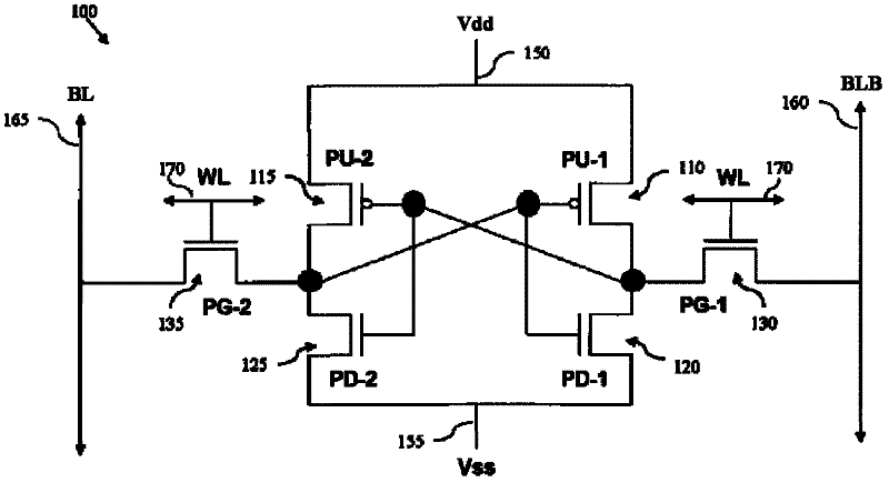
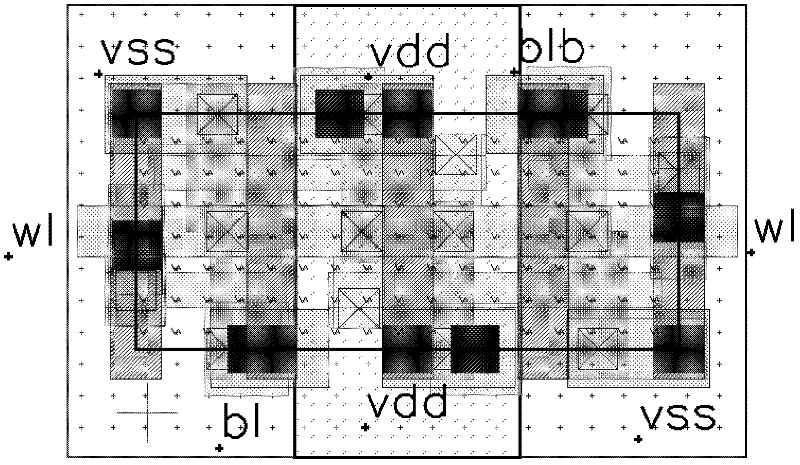
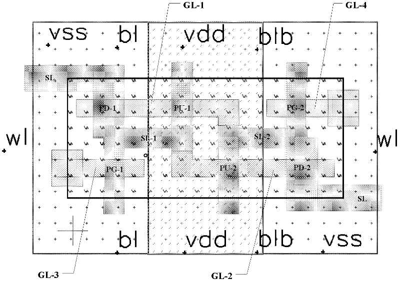
[0022] In order to make the above objects, features and advantages of the present invention more comprehensible, specific implementations of the present invention will be described in detail below in conjunction with the accompanying drawings.
[0023] The static random access memory formed on the SOI substrate provided by the present invention can be realized in various alternative ways, and the following is illustrated by a preferred embodiment. Of course, the present invention is not limited to this specific embodiment. Common substitutions known to those skilled in the art undoubtedly fall within the protection scope of the present invention.
[0024] Secondly, the present invention is described in detail using schematic diagrams. When describing the embodiments of the present invention in detail, for the convenience of illustration, the schematic diagrams are not partially enlarged according to the general scale, which should not be used as a limitation of the present inve...
PUM
 Abstract
Description
Claims
Application Information