Inverted LED light source

A technology of LED light source and LED chip, which is applied in the direction of electrical components, circuits, semiconductor devices, etc., can solve the problems of increasing heat transportation distance, reducing device reliability, increasing thermal resistance, etc., to improve chip yield and reduce thermal stress , The effect of reducing thermal resistance

Pending Publication Date: 2021-03-09
SUZHOU INST OF NANO TECH & NANO BIONICS CHINESE ACEDEMY OF SCI
View PDF0 Cites 2 Cited by
  • Summary
  • Abstract
  • Description
  • Claims
  • Application Information

AI Technical Summary

Problems solved by technology

[0003] For example, the existing flip-chip LED light source structure such as figure 1 As shown, however, due to the limitation of production technology, the processing accuracy of the metal layer spacing on the substrate is currently on the sub-micron level, and the spacing d1 of the PN electrodes on the existing chip is ≥ 150 μm; the schematic diagram of heat transfer is shown in figure 2 As shown, heat needs to be transported horizontally to the electrode area in the chip first, and then to the substrate vertically, which will increase the heat transport distance and thus increase the thermal resistance; in order to improve the heat dissipation capability and electrical conductivity of the chip, the metal layer of the substrate needs to have The size of the chip electrode matches, so the equipment needs to have high alignment accuracy during packaging. The alignment error of this structure is the distance between the PN electrodes, otherwise it will easily cause a short circuit; the chip will generate a lot of heat when it emits light, and the contact between the chip and the metal layer material Large area and different thermal expansion coefficients tend to generate thermal expansion stress on the contact surface, resulting in reduced device reliability

Method used


Image

  • Inverted LED light source
  • Inverted LED light source
  • Inverted LED light source

Examples


Embodiment 1

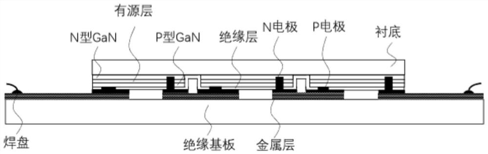
[0034] see image 3 and Figure 4 , a flip-chip LED light source, including a substrate 30 and at least one LED chip 10, the LED chip 10 is combined with the front surface of the substrate 30 with a first surface having electrodes, and the second surface of the LED chip 10 is a light-emitting surface and is opposite to the first surface. back to.

[0035] Wherein, the LED chip is a high-voltage and high-power integrated flip chip with good flatness, and the epitaxial layer of the LED chip 10 may include an N-type GaN layer 11, an active layer 12, and a P-type GaN layer formed on the substrate 20 in sequence. layer 13; further, an insulating layer 14 can also be provided on the epitaxial layer; the epitaxial layer is processed to form a plurality of unit cells arranged in an array, and the plurality of unit cells are connected in series and / or in parallel, each Each unit cell cooperates with a P electrode 15 and an N electrode 16, and the P electrode 15 and the N electrode 16...

Embodiment 2

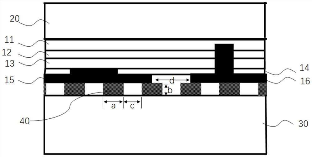
[0044] see Figure 5 , the structure of a flip-chip LED light source in this embodiment is basically the same as that of the flip-chip LED light source in Embodiment 1, the difference is that no external leads are provided on the front side of the insulating substrate 30 in this embodiment 60, and the conductive layer 53 and the conductive layer 54 are arranged at intervals on the back side of the insulating substrate 30, and the pad 51 and the pad 52 respectively pass through the conductive channel 31 and the conductive channel 32 of the substrate 30 to connect with the conductive layer 53 arranged on the back side of the substrate respectively. 1. The conductive layer 54 is electrically connected, so that electrical leads can be drawn out from the back of the insulating substrate. Both the conductive channel and the conductive layer can be made of metal, which is more conducive to timely transfer of the heat generated by the LED chip.

[0045] In some more specific embodime...


PUM


Abstract

The invention discloses an inverted LED light source, which comprises a substrate and at least one LED chip, and is characterized in that the LED chip is combined with the front surface of the substrate through a first surface with an electrode, and a second surface of the LED chip is a light emitting surface and is opposite to the first surface; and at least one pair of P electrodes and N electrodes of at least one LED chip are in heat conduction connection with the front face of the substrate through a plurality of heat conductors arranged at intervals, and the maximum size a of any heat conductor in the direction parallel to the first surface is smaller than the minimum distance d between the P electrodes and the N electrodes. According to the flip-chip LED light source provided by theinvention, a flip-chip bonding technology and a self-alignment isolation technology are combined, so that the chip yield is improved, and the thermal expansion stress of a welding interface is reduced; and meanwhile, the requirement on the alignment precision of equipment is reduced, so that the production cost is reduced, and the yield is improved.

Description

technical field [0001] The invention relates to an LED light source, in particular to a flip-chip LED light source, and belongs to the technical field of semiconductors. Background technique [0002] In flip-chip LEDs, in order to ensure that there is no short circuit between the PN electrodes of the chip when the chip is bonded, it is necessary to have a certain distance between the PN electrodes. On the other hand, in order to reduce the junction temperature, the contact area between the chip and the substrate needs to be as large as possible. , the pitch of the PN electrodes should be as small as possible, and traditional flip-chip technology usually requires devices to have high alignment accuracy, which will increase production costs. [0003] For example, the existing flip-chip LED light source structure such as figure 1 As shown, however, due to the limitation of production technology, the processing accuracy of the metal layer spacing on the substrate is currently o...

Claims


Application Information

Patent Timeline
Patent Type & Authority Applications(China)
IPC IPC(8): H01L33/64H01L33/62
CPCH01L33/62H01L33/642H01L33/647H01L33/64
Inventor 唐文婷蔡勇
Owner SUZHOU INST OF NANO TECH & NANO BIONICS CHINESE ACEDEMY OF SCI
Why Eureka
Try Eureka