Epitaxial structure of a light emitting diode and its manufacturing method

A technology of light-emitting diodes and epitaxial structures, applied in electrical components, circuits, semiconductor devices, etc., can solve the problem of low carrier mobility, and achieve the effects of improving recombination rate, improving brightness, and enhancing confinement effect.

Inactive Publication Date: 2011-12-28
XIAMEN CHANGELIGHT CO LTD
View PDF9 Cites 15 Cited by
  • Summary
  • Abstract
  • Description
  • Claims
  • Application Information

AI Technical Summary

Problems solved by technology

[0003] At present, the bright red and yellow light-emitting diodes mainly use multiple quantum well (multiple quantum well, MQW) structure as the active layer. Usually, light-emitting diodes emit energy through the recombination of electrons and holes in the quantum wells, so To improve the luminous efficiency of light-emitting diodes is mainly to increase the recombination rate of electrons and holes in the quantum well; The barrier heights of the barriers are the same, and the quantum barrier has a much stronger confinement effect on holes than electrons, so the recombination rate of electrons and holes in quantum wells is difficult to increase, which limits the brightness of light-emitting diodes

Method used


Image

  • Epitaxial structure of a light emitting diode and its manufacturing method
  • Epitaxial structure of a light emitting diode and its manufacturing method
  • Epitaxial structure of a light emitting diode and its manufacturing method

Examples


Embodiment Construction

[0023] The present invention will be described in further detail below in conjunction with the accompanying drawings and specific embodiments.

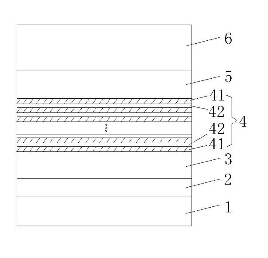
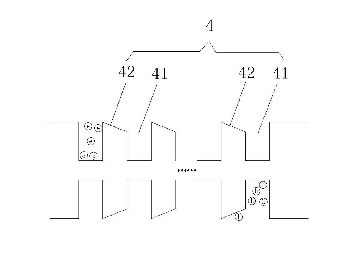
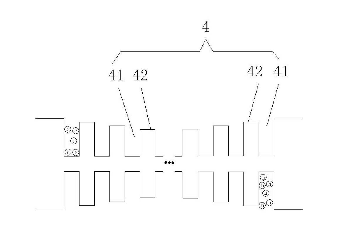
[0024] figure 1 As shown, an epitaxial structure of a light-emitting diode, on top of the GaAs substrate layer 1, there are Bragg reflection layer 2, first-type confinement layer 3, active layer 4, second-type confinement layer 5, and current spreading layer from bottom to top. Layer 6, the active layer 4 is composed of n groups of quantum wells 41 and quantum barriers 42 alternately, wherein the selection range of n is 100≥n≥2, so that the barrier height in the same quantum barrier 42 is a gradual change The distribution or the barrier heights between different quantum barriers 42 is a gradual distribution.

[0025] The above-mentioned epitaxial structure of the light-emitting diode can be manufactured through the following steps:

[0026] 1) Choose GaAs as the substrate layer;

[0027] 2) Growing a Bragg reflection layer on the b...


PUM


Abstract

The invention discloses an epitaxial structure of a light-emitting diode and a manufacturing method thereof. On a GaAs substrate layer, there are a Bragg reflection layer, a first-type confinement layer, an active layer, a second-type confinement layer, and a current spreading layer in sequence from bottom to top. , the active layer is composed of n sets of quantum wells and quantum barriers alternately, where 100≥n≥2, and the barrier height in the same quantum barrier is a gradual distribution or the barrier height between different quantum barriers It is a gradual distribution; its manufacturing method includes the following steps: select GaAs as the substrate layer, and grow a Bragg reflection layer, a first-type confinement layer, an active layer, a second-type confinement layer, and a current spreading layer sequentially on the GaAs substrate layer, wherein The active layer is formed by alternately growing n groups of quantum wells and quantum barriers, and the quantum barriers are made of (AlxGa1-x)yIn1-yP group III and V compounds, where 1≥x≥0.5, and the invention enhances the quantum barrier’s effect on electrons The confinement effect increases the recombination rate of electrons and holes in the quantum well, thereby increasing the brightness of the light-emitting diode.

Description

technical field [0001] The invention relates to the technical field of manufacturing the epitaxial structure of a light emitting diode, in particular to an epitaxial structure of an aluminum gallium indium phosphide light emitting diode and a manufacturing method thereof. Background technique [0002] Light-emitting diodes (LEDs) are gradually replacing traditional light sources due to their low power consumption, small size and high reliability. requirements. [0003] At present, the bright red and yellow light-emitting diodes mainly use multiple quantum well (multiple quantum well, MQW) structure as the active layer. Usually, light-emitting diodes release energy through the recombination of electrons and holes in the quantum wells, so To improve the luminous efficiency of light-emitting diodes is mainly to increase the recombination rate of electrons and holes in the quantum well; The barrier heights of the barriers are the same, and the quantum barrier has a much strong...

Claims


Application Information

Patent Timeline
Patent Type & Authority Applications(China)
IPC IPC(8): H01L33/06
Inventor 林志伟蔡建九陈凯轩林志园
Owner XIAMEN CHANGELIGHT CO LTD
Why Eureka
Try Eureka