
Multi-resistance-state resistance random access memory and method for implementing multiple resistance states utilizing same
A resistive memory, memory technology, applied in static memory, digital memory information, information storage, etc., can solve the problems of insufficient research on multi-value memory applications, low power consumption and process compatibility, and improve storage density and compatibility. Good, simple craftsmanship
- Summary
- Abstract
- Description
- Claims
- Application Information
AI Technical Summary
Problems solved by technology
Method used
Image

Examples
Embodiment Construction
[0026] A multi-resistance RRAM (also referred to as a multi-level RRAM) proposed by the present invention will be described in detail below with reference to the drawings and embodiments.
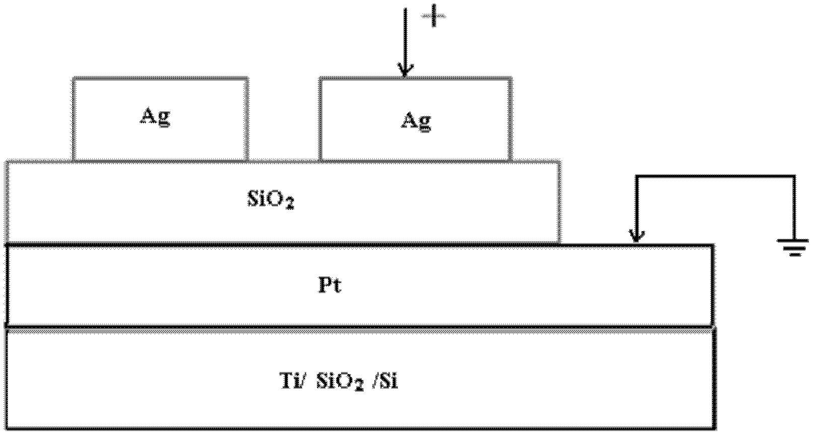
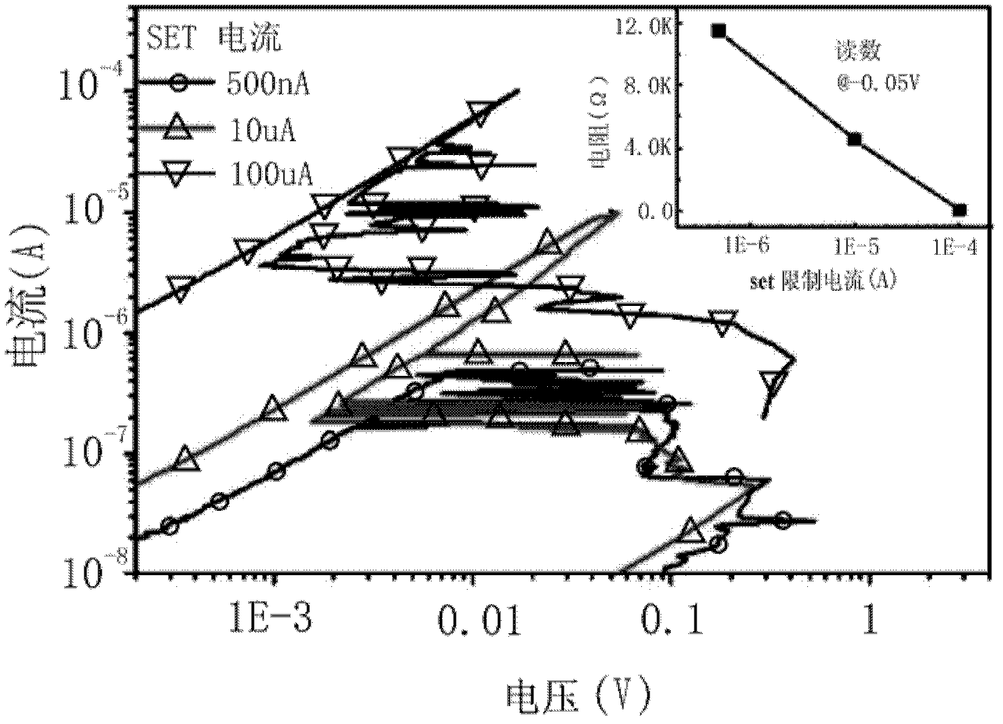
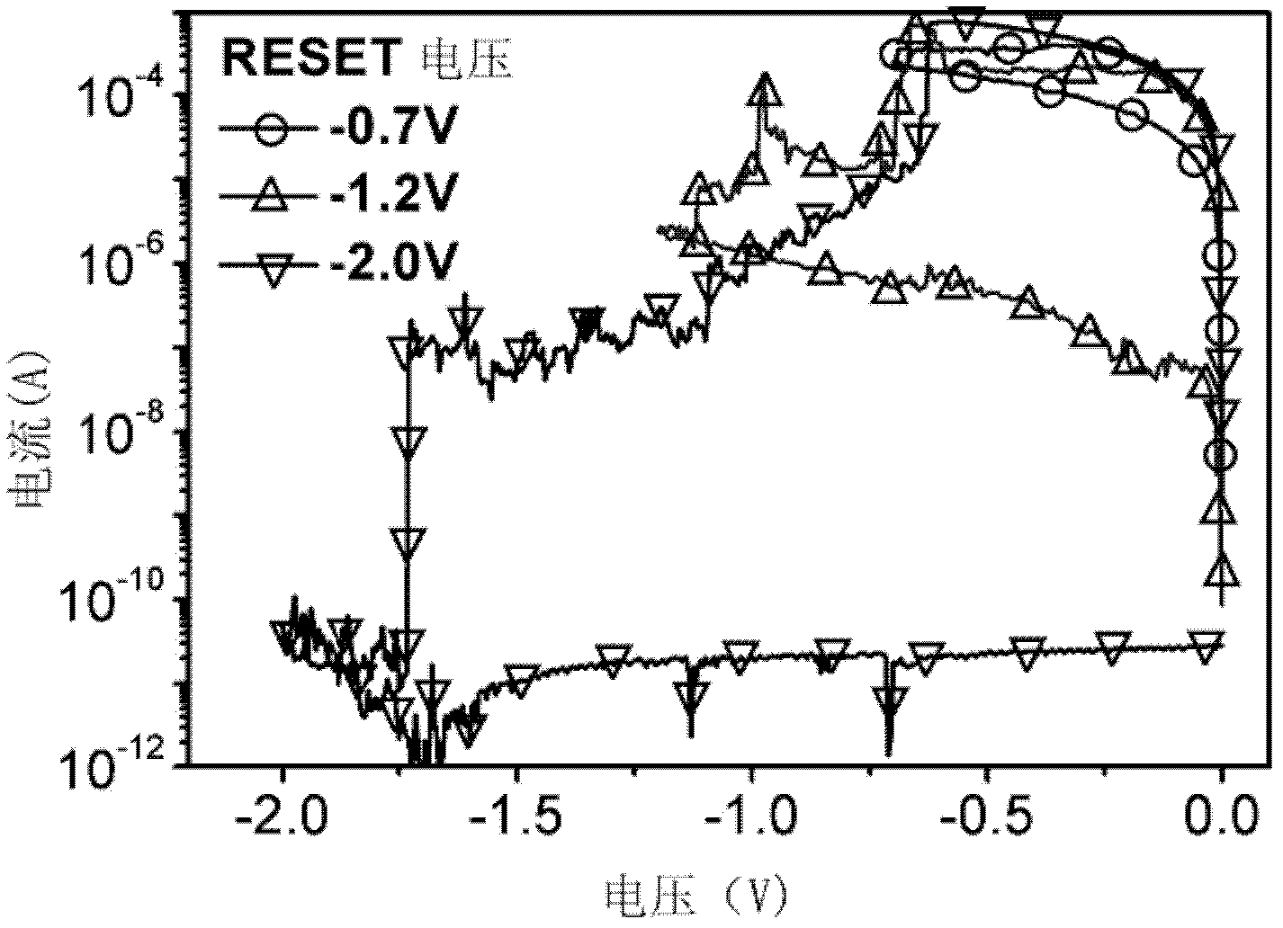
[0027] The multi-resistance resistive variable memory of the present invention is a MIM structure (MIM refers to a sandwich structure composed of metal, insulator, and metal three-layer film), including a top electrode (TE), a resistive variable layer (for oxide) and a bottom electrode ( BE). The metals of the top and bottom electrodes are prepared by sputtering, evaporation or MOCVD (metal organic compound chemical vapor deposition), SiO 2 Prepared by plasma-enhanced chemical vapor deposition. Such as figure 1 As shown, the embodiment of the present invention is Ag / SiO 2 / Pt / Ti / SiO 2 A multi-level resistance resistive memory device with / Si structure. Utilizing the bipolar resistance switching characteristics of the device, the resistance switching memory can generate four resistance ...
PUM
 Abstract
Description
Claims
Application Information