Method for estimating oxide semiconductor thin film and method for managing quality of oxide semiconductor thin film

A technology of oxide semiconductors and evaluation methods, applied in the direction of measuring electricity, measuring devices, measuring electrical variables, etc., to achieve accurate quality management, improve productivity, and improve yields

Active Publication Date: 2012-01-11
KOBE STEEL LTD
View PDF5 Cites 18 Cited by
  • Summary
  • Abstract
  • Description
  • Claims
  • Application Information

AI Technical Summary

Problems solved by technology

[0005] As a conventional evaluation method for the characteristics of semiconductor thin films, a gate insulating film and a passivation insulating film are usually formed on the semiconductor thin film to carry electrodes, and then characteristics such as mobility and threshold are measured. method, the time and cost required for the electrodes
In addition, by applying electrodes, new defects may be generated in the semiconductor thin film. From the viewpoint of further improving the manufacturing yield, it is required to establish a non-contact measurement method that does not require electrodes.

Method used


Image

  • Method for estimating oxide semiconductor thin film and method for managing quality of oxide semiconductor thin film
  • Method for estimating oxide semiconductor thin film and method for managing quality of oxide semiconductor thin film
  • Method for estimating oxide semiconductor thin film and method for managing quality of oxide semiconductor thin film

Examples


Embodiment 1

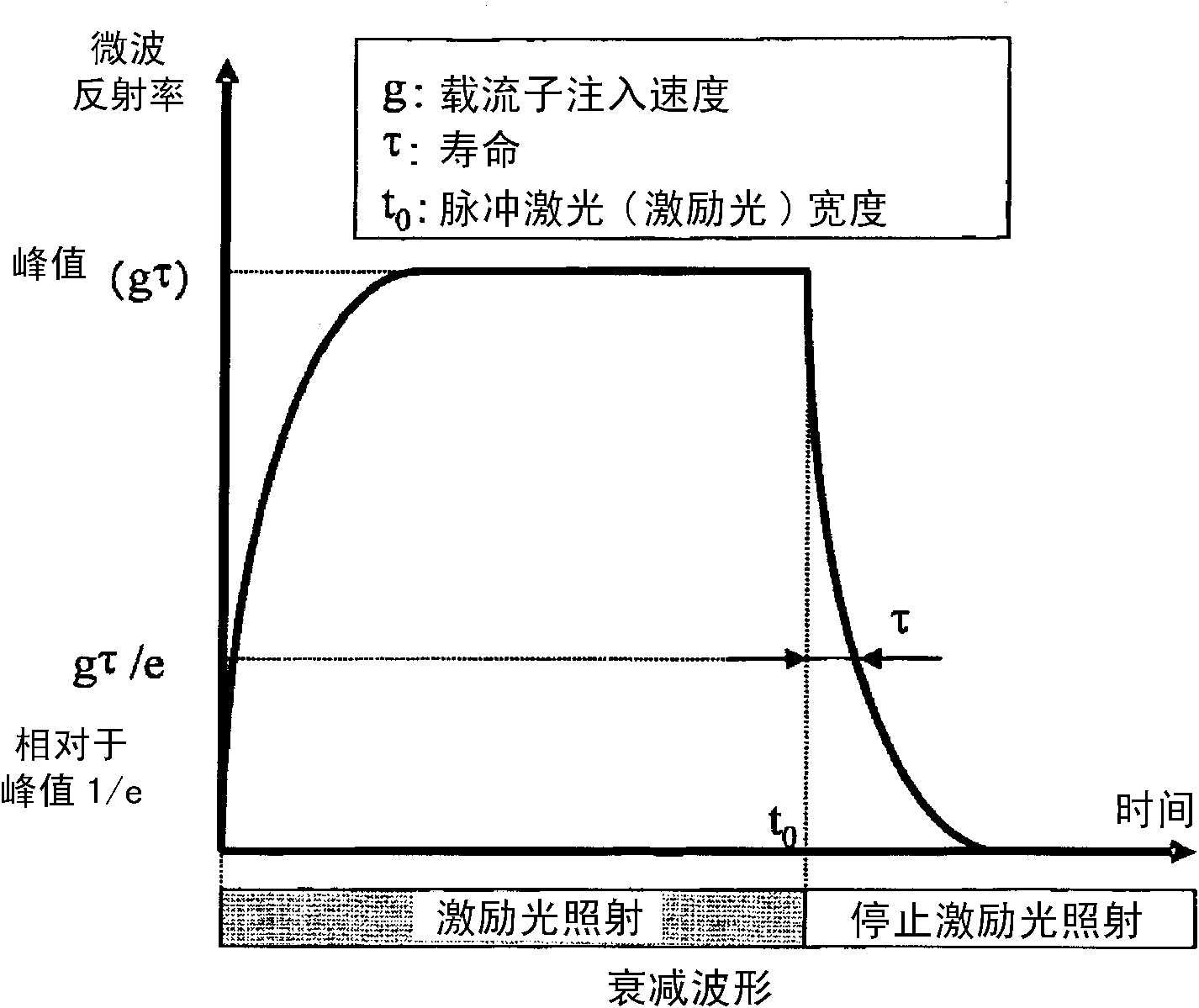
[0114] In Example 1, the correlation between the carrier mobility and the lifetime value or the peak value of the oxide semiconductor thin film was investigated by performing the following experiments.

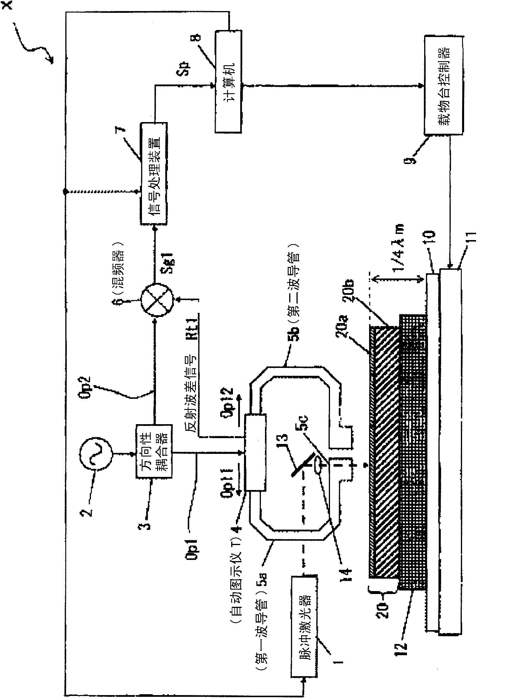
[0115] First, a sample of an amorphous oxide semiconductor thin film (InGaZnO) was produced for measuring lifetime by the microwave photoconductivity attenuation method. First, an oxide semiconductor thin film was formed by a sputtering method on a glass substrate (EAGLE2000 manufactured by Corning: 6 inches) under the following conditions.

[0116] Sputtering target composition: 1nGaZnO 4 (In:Ga:Zn=1:1:1)

[0117] Substrate temperature: room temperature

[0118] Film thickness of oxide semiconductor layer: 100nm

[0119] Oxygen addition amount: O 2 / (Ar+O 2 ) = 2%

[0120] Next, in order to change the mobility of the oxide semiconductor thin film, a pre-annealing treatment was performed under the following conditions to obtain a sample (Sample Ne. 1 was not subjected to...

Embodiment 2

[0150] In Example 2, the following oxide semiconductor thin film samples were produced in order to measure and evaluate the lifetime in-plane distribution of the sample using the microwave photoconductivity attenuation method (using the same apparatus as in Example 1).

[0151] The oxide semiconductor thin film was formed using the Co-Sputter method of simultaneously discharging two sputtering targets with different compositions. By fixing the substrate directly under the middle of the two sputtering targets, it is possible to form a thin film in which the amount of elements composed of the two sputtering targets is inclined in the surface of the substrate. In addition, the same glass plate as that of Example 1 was used as the substrate.

[0152] Co-sputter film formation conditions are as follows.

[0153] Sputtering target composition: ZnO, ZnSnO (the composition ratio of Zn:Sn is 3:2)

[0154] Substrate temperature: room temperature

[0155] Film thickness of the substra...

Embodiment 3

[0166] In Example 3, the following oxide semiconductor thin film samples were produced in order to determine and evaluate the in-plane distribution of the lifetime of the sample by the microwave photoconductivity attenuation method (using the same apparatus as in Example 1).

[0167] The oxide semiconductor thin film was formed using the Co-Sputter method in which three sputtering targets with different compositions were simultaneously discharged. By fixing the substrate directly under the middle of the three sputtering targets, a thin film in which the elemental amounts of the three sputtering targets are made up can be formed on the surface of the substrate. In addition, the same glass plate as that of Example 1 was used as the substrate.

[0168] Co-sputter film formation conditions are as follows.

[0169] Sputtering target composition: ZnO, ZnSnO (the composition ratio of Zn:Sn is 3:2), Al 2 o 3

[0170] Substrate temperature: room temperature

[0171]Film thickness ...


PUM


Abstract

The invention provides a method for estimating oxide semiconductor thin films and a method for managing the quality of oxide semiconductor thin films. The methods are applied for estimating and determining the electrical performances of the oxide semiconductor thin films in a non-contact and electrode-free way. The method comprises the steps of irradiating exciting light and microwave on samples equipped with oxide semiconductor thin films; stopping the irradiation of the exciting light after achieving the maximum value of the reflecting wave of the microwave from the oxide semiconductor thin film which is changed due to the irradiation of the exciting light; detecting the change of the reflectivity of the reflecting wave of the microwave from the oxide semiconductor thin film after the irradiation of the exciting light is stopped; and determining the mobility of the oxide semiconductor thin film according to the calculated service lifetime value derived from the detected value.

Description

technical field [0001] The present invention relates to an evaluation method of an oxide semiconductor thin film, and specifically relates to a method of determining and evaluating the carrier mobility of an oxide semiconductor thin film and a quality control method of an oxide semiconductor thin film. Background technique [0002] Semiconductors containing oxides such as indium (In), gallium (Ga), zinc (Zn), and tin (Sn) (oxide semiconductors) have semiconductor characteristics that are better as the field-effect mobility (mobility) is higher, so Applications to drive elements and the like for active matrix displays are being studied. In particular, oxide semiconductors can be formed into films at low temperatures and have a large optical band gap, so they can be formed into films on plastic substrates and film substrates, and applications to flexible displays and transparent displays using such substrates are being studied. [0003] However, in material development, it is...

Claims


Application Information

Patent Timeline
Patent Type & Authority Applications(China)
IPC IPC(8): G01R31/00
CPCG01N21/55G01N21/63G01N22/02
Inventor 钉宫敏洋安野聪森田晋也前田刚彰三木绫
Owner KOBE STEEL LTD
Why Eureka
Try Eureka