Method for preparing three-dimensional multivalue nonvolatile memory

A non-volatile memory technology, applied in the field of preparation of multi-valued non-volatile memory, can solve the problem of low storage density and achieve the effects of wide application, optimal programming, and increased storage density

Inactive Publication Date: 2012-01-11
INST OF MICROELECTRONICS CHINESE ACAD OF SCI
View PDF6 Cites 17 Cited by
  • Summary
  • Abstract
  • Description
  • Claims
  • Application Information

AI Technical Summary

Problems solved by technology

Patent US5825296 describes a three-dimensional structure read-only memory, and patent US20080023747 discloses the composition and preparation method of a semiconductor storage device array based on a multi-layer structure, but th

Method used


Image

  • Method for preparing three-dimensional multivalue nonvolatile memory
  • Method for preparing three-dimensional multivalue nonvolatile memory
  • Method for preparing three-dimensional multivalue nonvolatile memory

Examples


Embodiment Construction

[0027] In order to make the object, technical solution and advantages of the present invention clearer, the present invention will be described in further detail below in conjunction with specific embodiments and with reference to the accompanying drawings.

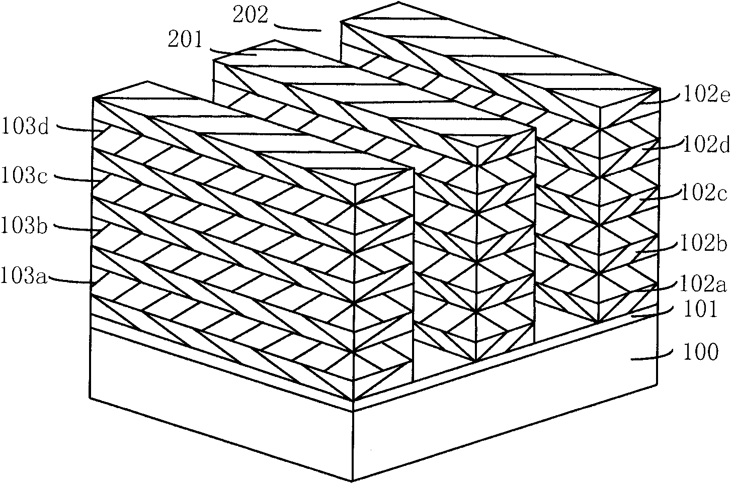
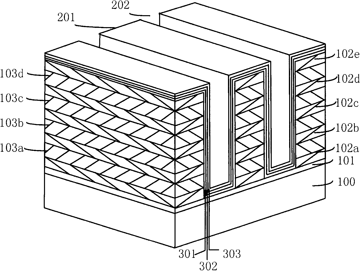
[0028] Figure 1 to Figure 10 is a schematic diagram of the preparation process used to illustrate an embodiment of the present invention.

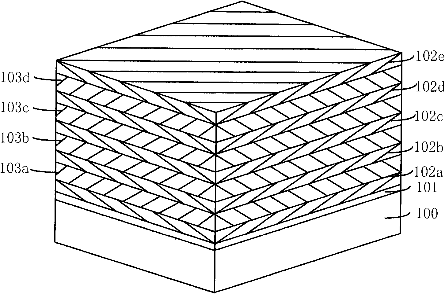
[0029] figure 1 It is the process of forming the gate stack structure on the semiconductor substrate in this embodiment. The semiconductor substrate 100 is a silicon wafer, a silicon germanium wafer, other similar semiconductor materials or a multilayer substrate material including an epitaxial silicon layer and a silicon germanium layer. The dielectric layer 101 is made of silicon dioxide or other materials with similar properties, and plays the role of buffer isolation. 102a, 102b, 102c, 102d, 102e are isolation dielectric layers made of silicon dioxide or other materials with s...


PUM


Abstract

The invention discloses a method for preparing a three-dimensional multivalue nonvolatile memory. The method comprises the following steps of: A, forming a grid lamination structure on a semiconductor substrate; B, forming a grid medium layer; C, forming a channel region and a source/drain doped region; and D, leading a bit line and a word line out of the source/drain doped region and a grid region so as to form three-dimensional integration of the nonvolatile memory. In the method, a plurality of physical storage points are obtained from a single device by comprehensively using a charge local storage property in a charge capture layer and a space characteristic of a vertical stack structure, so that multivalue storage is realized and the three-dimensional integration is formed on a storage device array; therefore, the storage density is increased basically. Meanwhile, the memory prepared by the method has higher device performance, namely programming, erasing, retaining and the like. The process for preparing the three-dimensional multivalue nonvolatile memory is compatible with the conventional silicon plane complementary metal oxide semiconductor (CMOS) process; the conventional storage device array structure integration can be adopted; and the method can be applied widely.

Description

technical field [0001] The invention relates to the technical fields of microelectronics manufacturing and memory, in particular to a method for preparing a multi-value non-volatile memory with three-dimensional integration characteristics and localized charge storage. Background technique [0002] The current microelectronics products are mainly divided into two categories: logic devices and storage devices, and storage devices are needed in almost all electronic products today, so storage devices occupy a very important position in the field of microelectronics. Storage devices can generally be classified into volatile memories and non-volatile memories. The main feature of non-volatile memory is the ability to retain stored information for a long period of time without power on. It not only has the characteristics of read-only memory (ROM), but also has high access speed, and is easy to erase and rewrite, and consumes less power. With the demand for large-capacity and l...

Claims


Application Information

Patent Timeline
IPC IPC(8): H01L21/8247
Inventor 刘明朱晨昕霍宗亮闫锋王琴龙世兵
Owner INST OF MICROELECTRONICS CHINESE ACAD OF SCI
Why Eureka
Try Eureka