Vertical fiber coupling module with multiple semiconductor lasers
A fiber coupling and semiconductor technology, applied in the field of vertical fiber coupling modules, can solve the problems of high manufacturing cost, difficult debugging, complicated wiring, etc., and achieve the effect of improving ease of use, tight arrangement, and convenient adjustment
- Summary
- Abstract
- Description
- Claims
- Application Information
AI Technical Summary
Problems solved by technology
Method used
Image
Examples
Embodiment 1
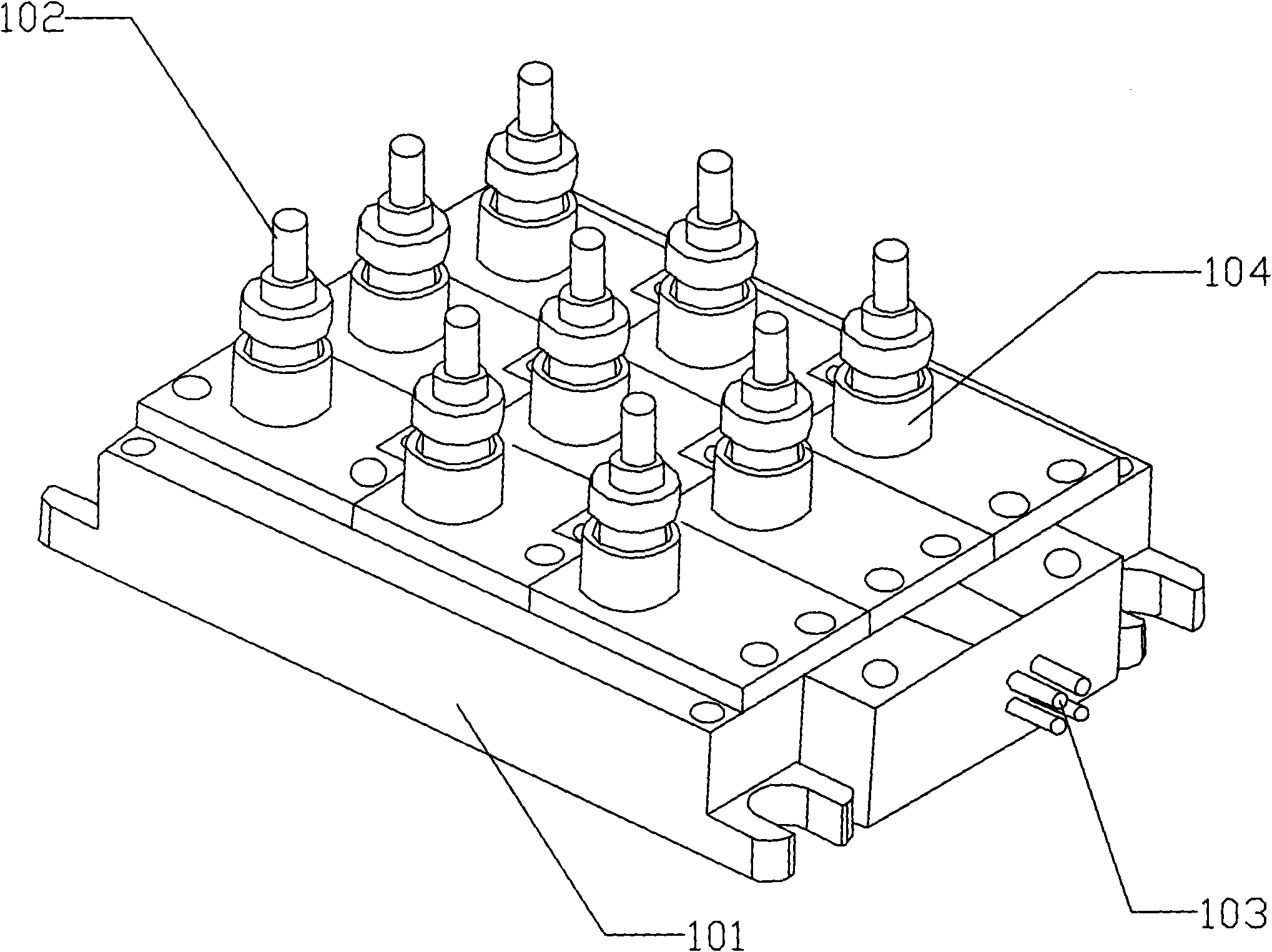
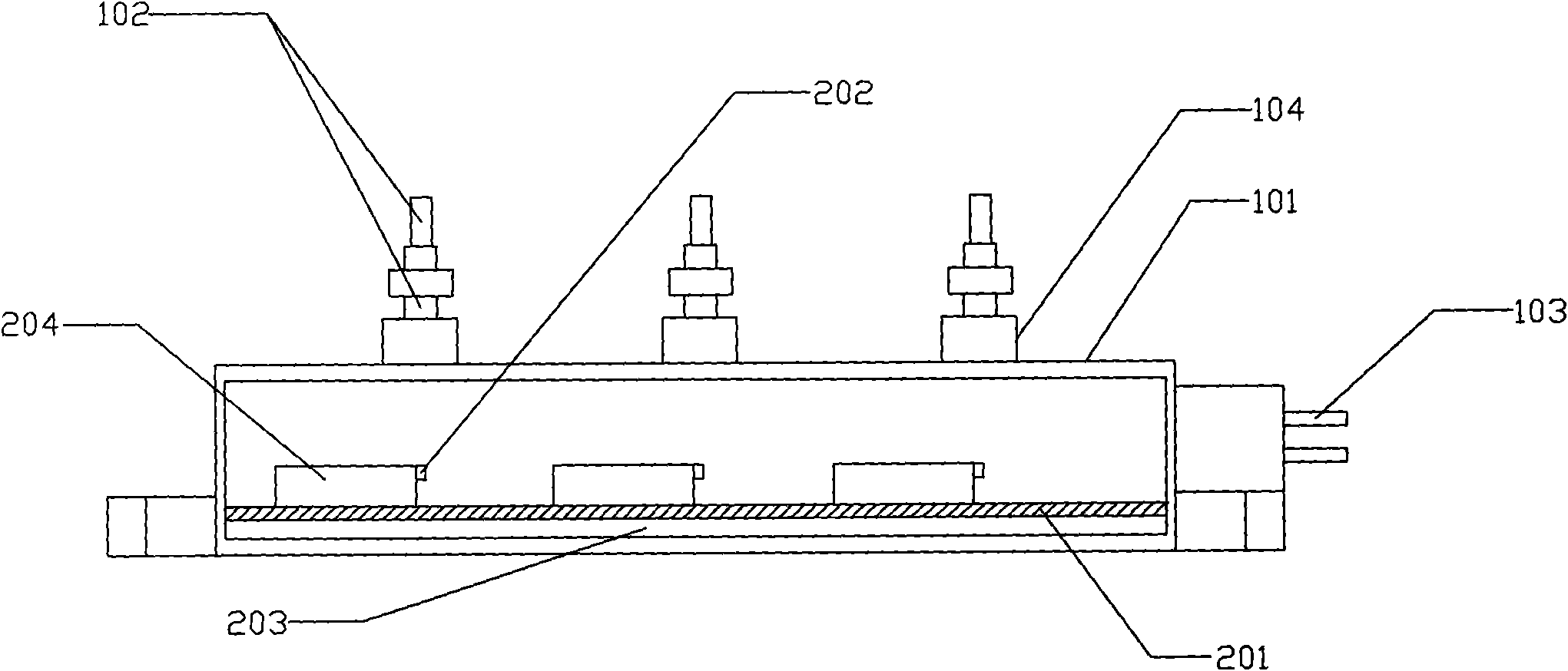
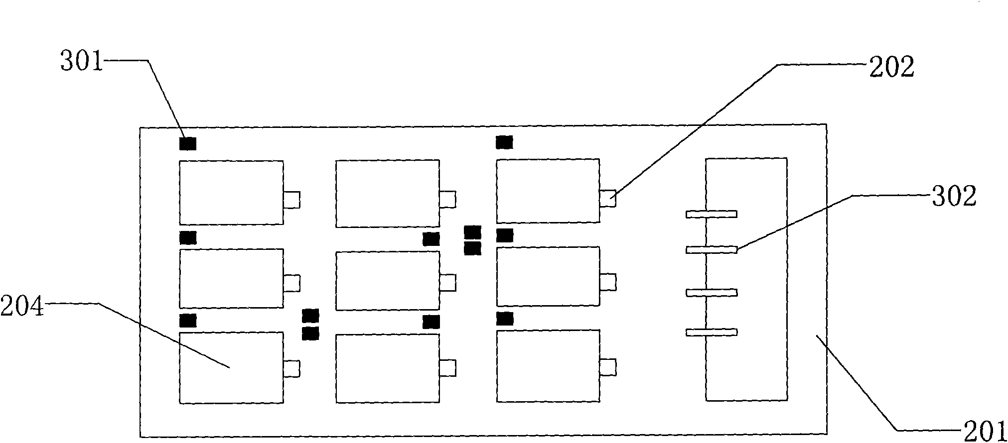
[0039] see figure 1 As shown, the vertical fiber coupling module of multiple semiconductor lasers includes a packaging case 101 and nine fixing tubes 104 opened on the top of the packaging case 101 . Such as figure 2 , image 3 As shown, a lens-fiber assembly 102 is arranged in each fixing tube 104, and nine semiconductor lasers 202 coaxial with the lens-fiber assembly 102 and a heat sink 204 for fixing the semiconductor laser 202 are arranged in the package housing 101 , for fixing the heat sink 204 and electrically connecting the substrate 201 of the semiconductor laser 202 , the semiconductor laser 202 is fixed on the substrate 201 through the heat sink 204 . The axes of the lens-fiber assembly 102 and the semiconductor laser 202 are perpendicular to the plane where the substrate 201 is located, and the laser light emitted by the semiconductor laser 202 is vertical to the substrate 201 and incident on the lens-fiber assembly 102 upwards, and the laser light is emitted a...
Embodiment 2
[0045] see Figure 5 As shown, the vertical fiber coupling module of a plurality of semiconductor lasers includes a packaging case 101 and nine mounting holes 501 opened on the top of the packaging case 101, and a lens-fiber assembly 102 is arranged in each mounting hole 502, and the packaging case 101 is provided with nine semiconductor lasers 202 coaxial with the lens-fiber assembly 102, a heat sink 204 for fixing the semiconductor lasers 202, a substrate 201 for fixing the heat sinks 204 and electrically connecting the semiconductor lasers 202, and the semiconductor lasers 202 pass through The heat sink 204 is fixed on the substrate 201 . The axes of the lens-fiber assembly 102 and the semiconductor laser 202 are perpendicular to the plane where the substrate 201 is located, and the laser light emitted by the semiconductor laser 202 is vertical to the substrate 201 and incident on the lens-fiber assembly 102 upwards, and the laser light is emitted at one end of the semicond...
Embodiment 3
[0050] The main structure is the same as that of Embodiment 1, the difference is that four semiconductor lasers 202 are arranged on the substrate 201, such as Figure 7 As shown, the substrate is provided with a solder joint 301 and a stitch solder joint 302 for conducting the semiconductor laser 202 .
[0051] The dimensions and distances of the components in all the drawings in the present invention are for illustration purposes and not for limitation, and the specific application process will be different from them.
PUM
 Abstract
Description
Claims
Application Information


