

White light photonic crystal with nanometer micro lens array and preparation method thereof
A technology of photonic crystals and microlenses, applied in light guides, optics, optical components, etc., can solve the problems of long processing time and high defect rate of photonic crystals
- Summary
- Abstract
- Description
- Claims
- Application Information
AI Technical Summary
Problems solved by technology
Method used
Image

Examples
no. 1 example
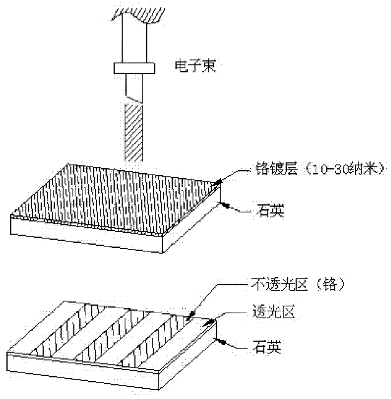
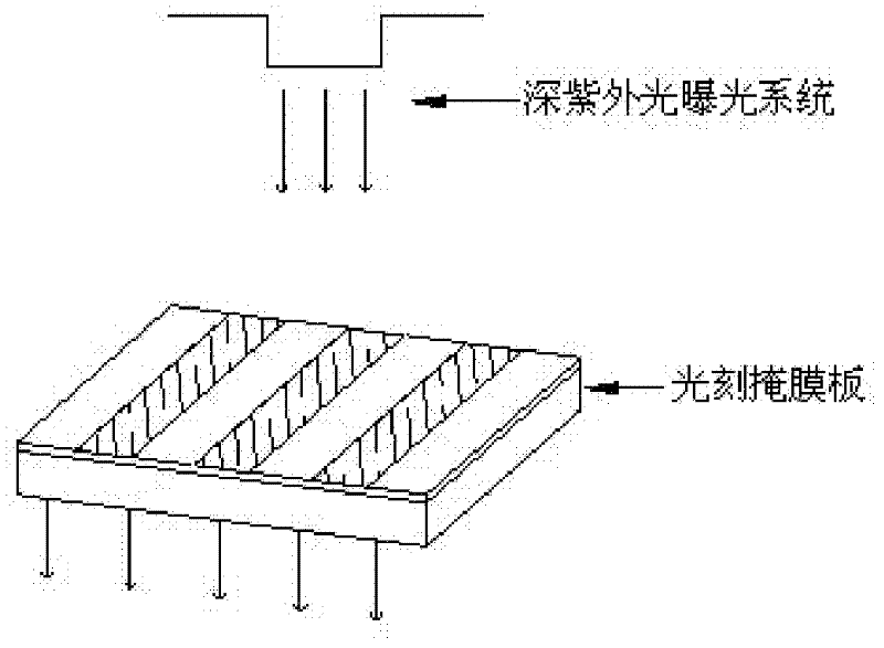
[0018] According to the first embodiment of the present invention, there is provided a structure of a white light photonic crystal having a nano-microlens array, the structure comprising: a patterned quartz material photolithography mask (Photo mask), on which a chromium metal layer is arranged; The photolithographic mask plate is coated with a negative photoresist; a nickel-iron alloy plating solution (nickel-iron ratio of 7-9:3-1) is arranged on it to form a metal mask layer with nanoscale microlenses; metal In the pattern arrangement of the shielding layer, the red, green and blue three-color transparent fluorescent glue that is baked to form red, green and blue three-color nano-micro-lenses is arranged, and the red, green and blue three-color transparent fluorescent glue is printed on the metal mask (Metal mask) layer. Multiple quantum wells.
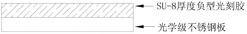
[0019] Among them, the thickness of the chromium metal layer is 10-30 nanometers; the negative photoresist (Negative photo resist)...
PUM
| Property | Measurement | Unit |
|---|---|---|
| thickness | aaaaa | aaaaa |
| thickness | aaaaa | aaaaa |
| thickness | aaaaa | aaaaa |
Abstract
Description
Claims
Application Information