High-reliability split-gate nonvolatile memory structure with high-speed low-voltage operation function

A non-volatile, high-speed and low-voltage technology, applied in semiconductor devices, electro-solid devices, electrical components, etc., it can solve problems such as mismatch of electron and hole injection positions, aggravation of mismatch, and degradation of data retention time, reducing programming. voltage, achieve uniform distribution, and improve the effect of impact ionization rate

Active Publication Date: 2012-02-01
宁夏储芯科技有限公司
View PDF8 Cites 11 Cited by
  • Summary
  • Abstract
  • Description
  • Claims
  • Application Information

AI Technical Summary

Problems solved by technology

However, this method of operation faces reliability problems, as follows: When the SSI realizes the programming operation, the electronics will mainly be concentrated in the figure 2 The location of the storage layer in the dotted line is different from the floating gate structure which is an equipotential body. This charge trap storage structure makes the density of electrons in the storage layer near the source much higher than that in the storage layer near the drain.
However, when HHI is used for erasing, the distribution of holes in the entire storage layer structure is relatively uniform, so there is an obvious mismatch between the injection positions of electrons and holes.
After multiple programming and erasing operations, the mismatch between charges and holes in the storage layer will intensify, thereby degrading device characteristics (such as channel threshold voltage distribution, data retention time, etc.)

Method used


Image

  • High-reliability split-gate nonvolatile memory structure with high-speed low-voltage operation function
  • High-reliability split-gate nonvolatile memory structure with high-speed low-voltage operation function
  • High-reliability split-gate nonvolatile memory structure with high-speed low-voltage operation function

Examples


Embodiment Construction

[0030] In order to make the object, technical solution and advantages of the present invention clearer, the present invention will be described in further detail below in conjunction with specific embodiments and with reference to the accompanying drawings.

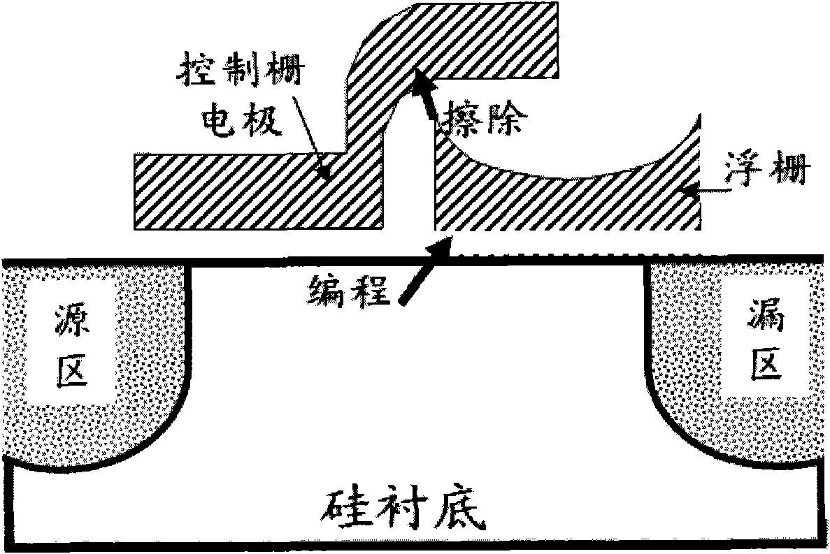
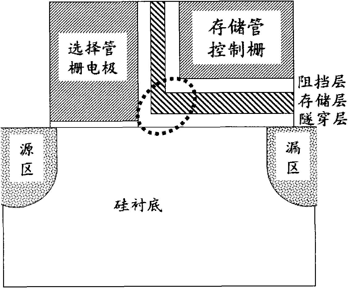
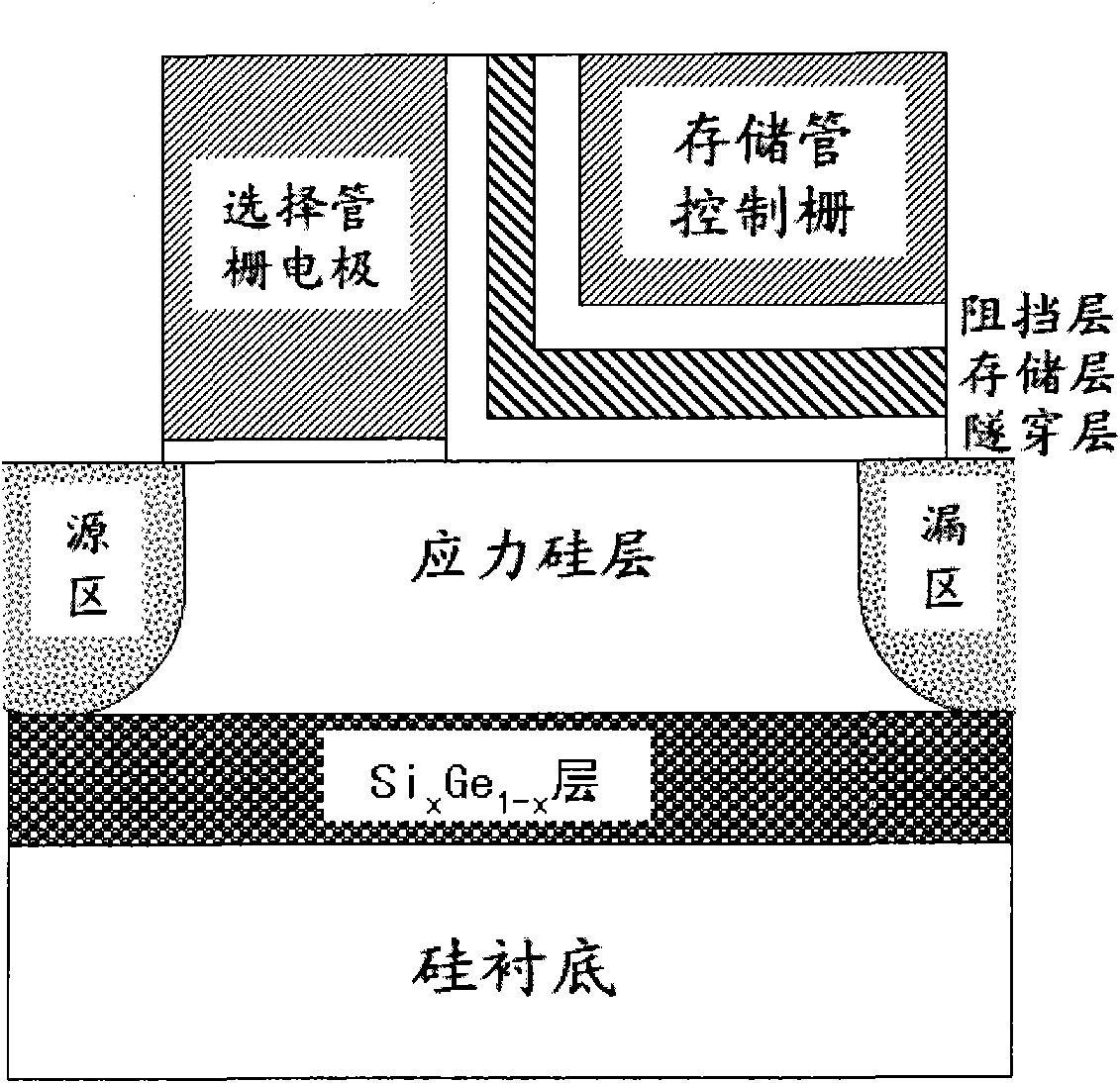
[0031] Such as image 3 , 4 As shown in and 5, the highly reliable split-gate non-volatile memory structure with high-speed and low-voltage operation provided by the present invention includes a selection transistor and a memory transistor, and the selection transistor and the memory transistor share the substrate region and source-drain doping area, while memory transistors have a stack structure, and information is stored in the charge storage layer below the gate area. The preparation method and the required process are compatible with the traditional process.

[0032] Wherein, the substrate region shared by the selection transistor and the memory transistor is a double-layer structure or a multi-layer structure comp...


PUM


Abstract

The invention discloses a high-reliability split-gate nonvolatile memory structure with a high-speed low-voltage operation function, which is characterized in that the structure comprises a selection transistor and a memory transistor, the selection transistor and the memory transistor share a substrate region and a source / drain doped region, the memory transistor is provided with a stack structure and information is stored in a charge storage layer below a grid region. By adopting a dual-layer or multilayer substrate made of stress silicon / germanium-silicon and by comprehensively utilizing high collision ionization rate brought by primary collision ionization of the channels of the stress silicon, high collision ionization rate brought by the introduction of a SixGel-x layer and wider transverse electron distribution produced resultantly, the programming efficiency of a split-gate structure can be greatly improved, the programming voltage is reduced, the data hold characteristic of adevice is improved and the high-reliability operation of the device is facilitated. Since the charge-trap-type split-gate memory preparation process disclosed by the invention is compatible with the traditional silicon planar complementary metal oxide semiconductor (CMOS) process, the wide application is facilitated.

Description

technical field [0001] The invention relates to the technical field of microelectronics manufacturing and memory, in particular to a highly reliable split-gate non-volatile memory structure with high-speed and low-voltage operation. Background technique [0002] The current microelectronics products are mainly divided into two categories: logic devices and storage devices, and storage devices are needed in almost all electronic products today, so storage devices occupy a very important position in the field of microelectronics. Storage devices can generally be classified into volatile memories and non-volatile memories. The main feature of non-volatile memory is the ability to retain stored information for a long period of time without power on. It not only has the characteristics of read-only memory (ROM), but also has high access speed, and is easy to erase and rewrite, and consumes less power. With the demand for large-capacity and low-power storage in multimedia applic...

Claims


Application Information

Patent Timeline
Patent Type & Authority Applications(China)
IPC IPC(8): H01L27/115H01L29/06H01L27/1157
Inventor 霍宗亮刘明
Owner 宁夏储芯科技有限公司
Why Eureka
Try Eureka