DMOS device and manufacturing methods thereof

A manufacturing method and device technology, applied in semiconductor/solid-state device manufacturing, semiconductor devices, electrical components, etc., to achieve the effects of increasing doping concentration, improving conduction breakdown voltage, and widening the safe working area

Active Publication Date: 2012-02-01
SHANGHAI HUAHONG GRACE SEMICON MFG CORP
View PDF4 Cites 3 Cited by
  • Summary
  • Abstract
  • Description
  • Claims
  • Application Information

AI Technical Summary

Problems solved by technology

Therefore, in the optimization of the off-state breakdown voltage, on-state breakdown voltage and on-resistance of DMOS, the doping requirements for the drift region are contradictory, which is also the main constraint factor for the optimization of conventional DMOS characteristics.

Method used


Image

  • DMOS device and manufacturing methods thereof
  • DMOS device and manufacturing methods thereof
  • DMOS device and manufacturing methods thereof

Examples


Embodiment 1

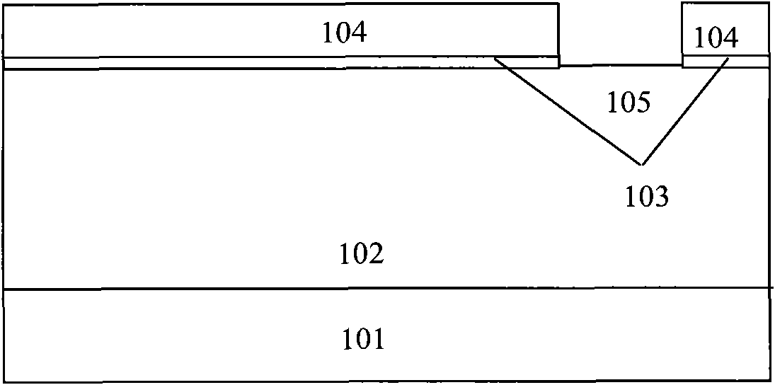
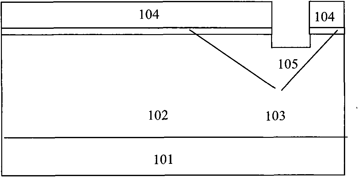
[0027] Such as Figure 1 to Figure 5 As shown, it is a schematic diagram of the device structure in each step of a DMOS device manufacturing method according to the embodiment of the present invention. Embodiment 1 DMOS device manufacturing method of the present invention comprises the following steps:

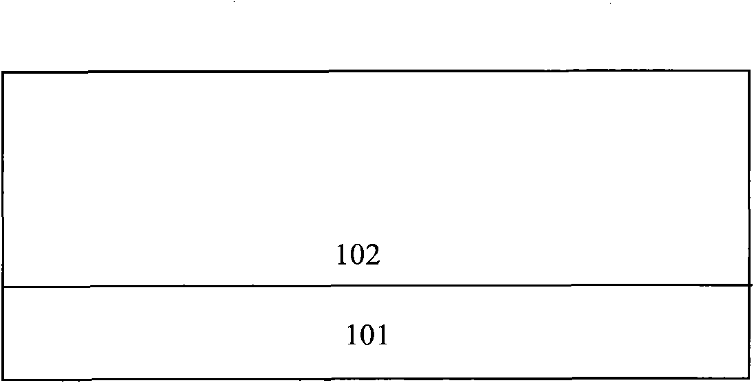
[0028] Step 1, such as figure 1 As shown, multiple second conductivity type ion implantations are performed on the first conductivity type silicon substrate 101, and the implantation energy of the second conductivity type multiple ion implantations is gradually reduced according to the order of implantation, and finally a light doping drift is formed. region 102 , where the impurity implanted with ions with low implantation energy is at the upper position of the lightly doped drift region 102 . For N-type DMOS, the implantation impurity for multiple ion implantations of the second conductivity type is phosphorus or arsenic, the implantation energy is 10KeV-1500KeV, and the ...

Embodiment 2

[0033] Such as Figure 6 to Figure 10 Shown is a schematic diagram of the device structure in each step of the DMOS device manufacturing method in Embodiment 2 of the present invention. The second DMOS device manufacturing method of the present invention includes the following steps:

[0034] Step 1, such as Figure 6 As shown, the first ion implantation of the second conductivity type is performed on the substrate 201 of the first conductivity type to form a lightly doped drift region 202 ; an isolation oxide layer is formed, and the lightly doped drift region 202 is thermally advanced. For N-type DMOS, the impurity implanted in the first ion implantation is phosphorus or arsenic, the implantation energy is 10KeV-1500KeV, and the implantation dose ranges from 1e11cm -2 ~1e13cm -2 . For P-type DMOS, the implanted impurity for the first ion implantation is boron, the implantation energy is 5KeV-1000KeV, and the implantation dose range is 1e11cm -2 ~1e13cm -2 . The isolat...

Embodiment 40V

[0039] Such as Figure 5 As shown, the DMOS device of the embodiment of the present invention realizes the high breakdown voltage of the DMOS device through the drift region under the local field oxygen isolation oxide layer 106, that is, the lightly doped drift region 105, that is, the cut-off breakdown voltage of the DMOS device can be maintained. unchanged or improved; and through the drift region of the active region, that is, the improvement of the doping concentration of the middle-doped drift region 107 between the channel region 108 and the local field oxygen isolation oxide layer 106, it can effectively improve The on-breakdown voltage of the DMOS can also reduce the on-resistance of the DMOS and widen the safe working area of ​​the DMOS. The main theoretical basis is: since the drift region mainly relies on the region under the isolation oxide layer, namely the lightly doped drift region 105 for voltage division, light doping is required to ensure a high breakdown vo...


PUM


Abstract

The invention discloses a DMOS device. Lateral impurities in a drift region distribute nonuniformly and drift region impurity concentration of an active region is greater than the drift region impurity concentration under an isolated oxidation layer. The invention discloses a manufacturing method of the DMOS device. The method comprises the following steps: carrying out several times of ion implantation from high energy to low energy in an area of forming the drift region; carrying out silicon etching in the area of forming the isolated oxidation layer; forming the isolated oxidation layer and carrying out heat propulsion to the drift region. The invention discloses another manufacturing method of the DMOS device. The method comprises the following steps: carrying out first ion implantation so as to form a lightly doped drift region and the isolated oxidation layer, and then carrying out the heat propulsion to the lightly doped drift region; carrying out the second ion implantation, wherein injection energy of the second ion implantation is less than the injection energy of the first ion implantation; carrying out impurity heat propulsion. By using the device and the methods of the invention, on-resistance can be reduced; a high injection effect can be decreased; a conduction breakdown voltage can be increased; a cut-off breakdown voltage of the device can be maintained or raised.

Description

technical field [0001] The invention relates to the field of manufacturing semiconductor integrated circuits, in particular to a DMOS device, and also relates to a method for manufacturing the DMOS device. Background technique [0002] High-voltage DMOS is one of the important devices in the BCD (Bipolar-CMOS-DMOS) process. The important standards of its characteristics are breakdown voltage (including off-state breakdown voltage and on-state breakdown voltage) and on-resistance. DMOS Device optimization mainly revolves around improving breakdown voltage and reducing on-resistance. The improvement of the off-state breakdown voltage and the reduction of the hot electron effect can be achieved by reducing the doping concentration of the drift region, but the improvement of the on-state breakdown voltage must be achieved by appropriately increasing the doping of the drift region and reducing the large injection effect. The most effective way to reduce the on-resistance is to i...

Claims


Application Information

Patent Timeline
Patent Type & Authority Applications(China)
IPC IPC(8): H01L29/78H01L29/36H01L21/336
CPCH01L29/0878H01L29/42368H01L29/66681H01L29/7816
Inventor 钱文生
Owner SHANGHAI HUAHONG GRACE SEMICON MFG CORP
Why Eureka
Try Eureka