Probe of conducting atomic force microscope and measuring methods employing probe

An atomic force microscope and atomic force technology, applied in the measurement of electricity, measurement devices, measurement of electrical variables, etc., can solve the problems of difficult to meet the needs of micro-nano structure detection and limited enhancement effect of the needle tip.

Active Publication Date: 2012-02-15
SUZHOU INST OF NANO TECH & NANO BIONICS CHINESE ACEDEMY OF SCI
View PDF2 Cites 56 Cited by
  • Summary
  • Abstract
  • Description
  • Claims
  • Application Information

AI Technical Summary

Problems solved by technology

However, using ordinary metal-coated atomic force microscope probes, because their plasmon oscillation frequencies are far away from the terahertz frequency, the tip enhancement effect is limited.
This makes its spatial resolution better than the diffraction limit, but it is still difficult to meet the needs of micro-nanostructure detection
In both of the above applications, AFM probes coated with conventional thin metal films show limitations

Method used


Image

  • Probe of conducting atomic force microscope and measuring methods employing probe
  • Probe of conducting atomic force microscope and measuring methods employing probe
  • Probe of conducting atomic force microscope and measuring methods employing probe

Examples


Embodiment Construction

[0010] A specific embodiment of a probe for a conductive atomic force microscope provided by the present invention and a measurement method using the probe will be described in detail below in conjunction with the accompanying drawings.

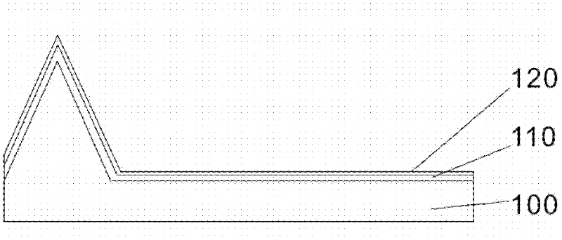
[0011] attached figure 1 Shown is a schematic structural view of the probe of the conductive atomic force microscope according to the specific embodiment of the present invention, including a substrate 100 , a nickel film 110 and a graphene film 120 . The probe can be prepared by plating a nickel film 110 with a thickness of 5-50 nm on the surface of the cantilever probe substrate 100 used in the atomic force microscope by thermal evaporation or magnetron sputtering. This metallization method belongs to the known technology and will not be described in detail here. The nickel film 110 is a catalyst layer for growing graphene on the probe, so its material can also be other metals, and the material of the cantilever probe base can be silicon, ...


PUM


Abstract

The invention relates to a probe of a conducting atomic force microscope. The probe comprises: a substrate of a cantilever probe; a needle tip; and a conductive film, which is arranged at a surface of the needle tip. Besides, the material of the conductive film is graphene. Moreover, the invention provides a method that employs the probe to measure local conductivity of a semiconductor and a needle tip-free near-field optical detection method that employs the probe to measure a terahertz wave band. According to the invention, graphene is utilized, wherein the grapheme has the following characteristics that: the graphene is composed of carbon atoms and is thin to a monatomic layer; and the graphene is a semimetal two-dimensional thin material that has a zero gap; besides, the probe has advantages of good conductivity and high electron mobility; moreover, a Fermi surface can carry out self-adjustment with charging and discharging motions and a carrier injection potential is low. In addition, an electronic plasmon oscillating frequency of the graphene is just at a terahertz wave band; and the graphene has soft materials and strong stability on thermodynamics. The above-mentioned statements are physical bases on which the graphene is utilized to replace a traditional metal material as a plated film of a surface of an atomic force microscope probe, so that the above-mentioned limitations are broken through.

Description

technical field [0001] The invention relates to the technical field of semiconductor material testing, in particular to a probe of a conductive atomic force microscope and a measuring method using the probe. Background technique [0002] The basic function of an atomic force microscope is to perform high-precision imaging at the micro-nano scale on the surface topography of samples such as conductors, semiconductors, and insulators. In addition, with the help of depositing metal and other conductive films on the surface of the cantilever probe of the atomic force microscope, the electrical and optical properties of the micro- and nanoscale micro-regions on the sample surface can also be tested and analyzed as follows: First, the conductive atomic force microscope mode, in the probe A bias voltage is applied between the metal coating of the needle and the sample, so that a current is generated when the probe and the sample surface are in contact. By measuring the relationship...

Claims


Application Information

Patent Timeline
Patent Type & Authority Applications(China)
IPC IPC(8): G01Q60/40G01R31/00
Inventor 徐耿钊刘争晖钟海舰樊英民徐科
Owner SUZHOU INST OF NANO TECH & NANO BIONICS CHINESE ACEDEMY OF SCI
Why Eureka
Try Eureka