Photovoltaic inverter IGBT (Insulated Gate Bipolar Transistor) heat-dissipating structure
A photovoltaic inverter, heat dissipation structure technology, applied in photovoltaic power generation, conversion of irreversible DC power input to AC power output, cooling/ventilation/heating transformation, etc. Problems such as low heat conduction efficiency, to achieve the effect of increasing circuit design cost and use cost, good heat dissipation effect, and improving efficiency
- Summary
- Abstract
- Description
- Claims
- Application Information
AI Technical Summary
Problems solved by technology
Method used
Image
Examples
Embodiment 1
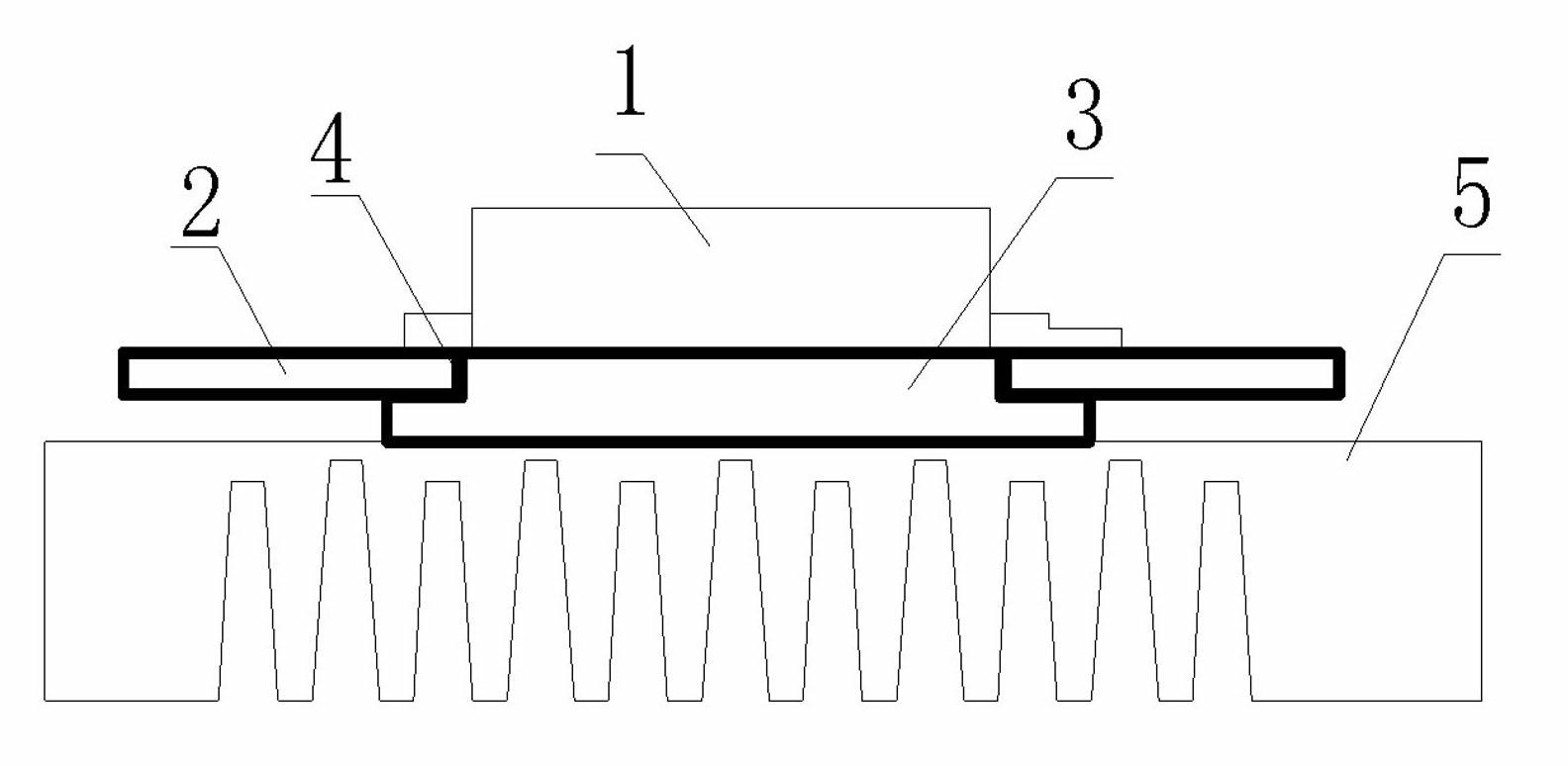
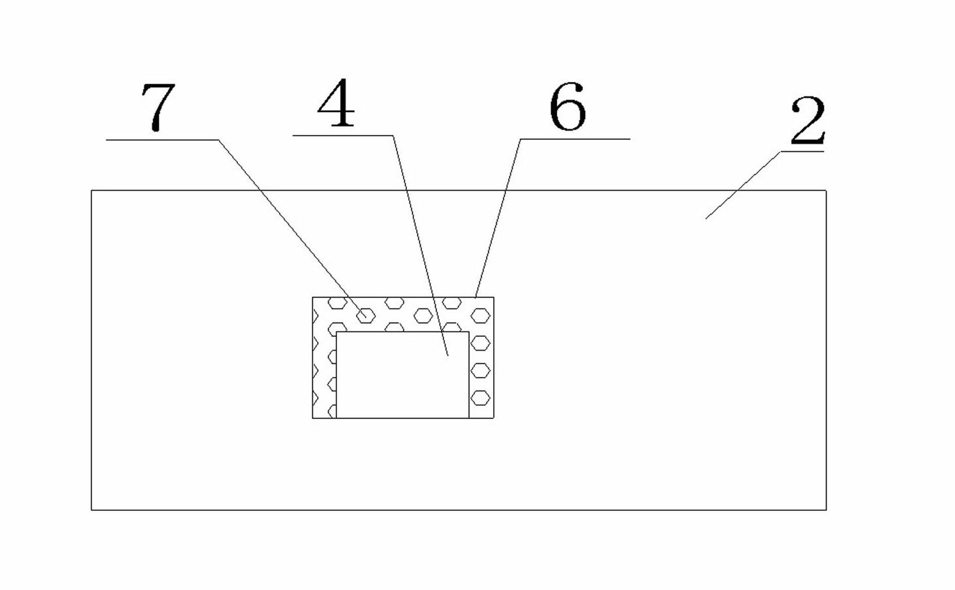
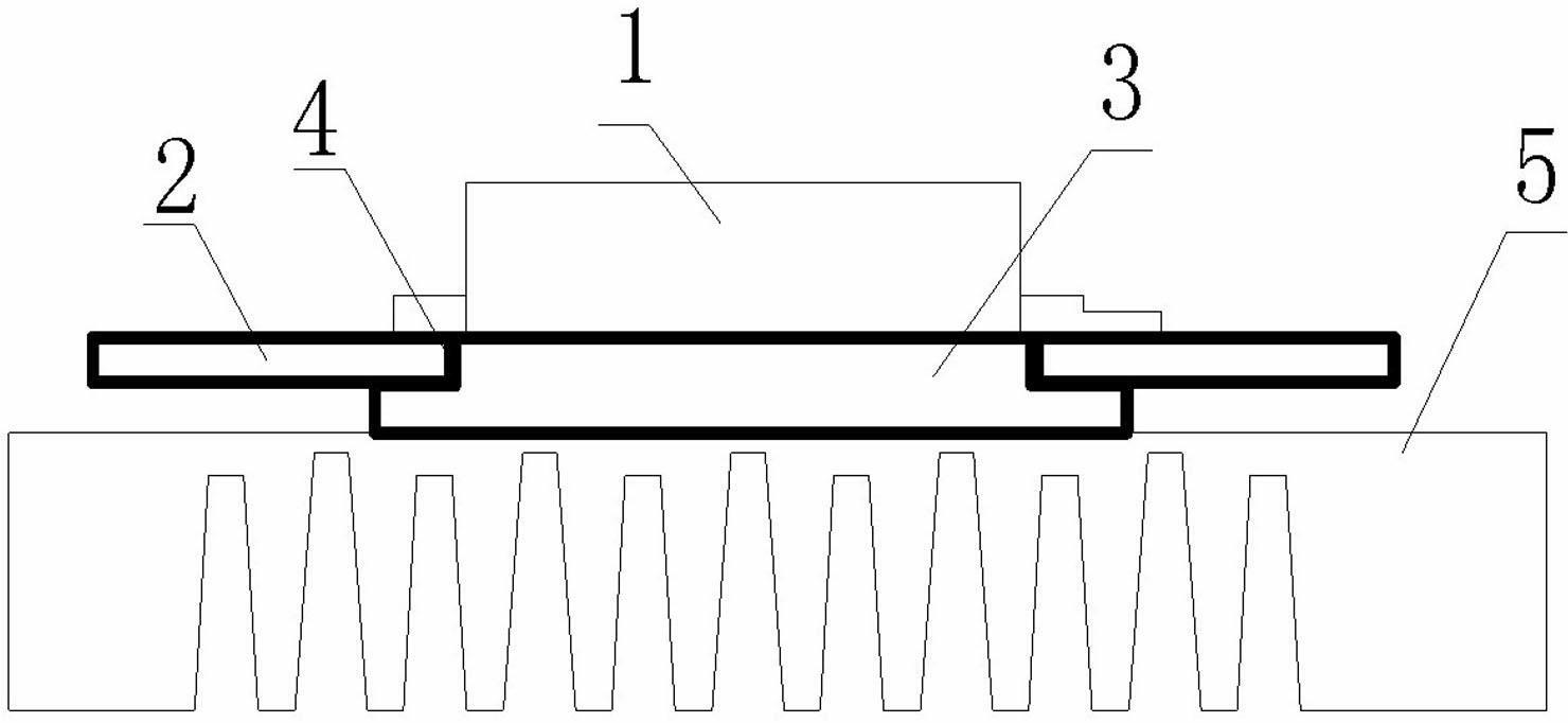
[0019] Embodiment one: see figure 1 , figure 2 . The photovoltaic inverter IGBT heat dissipation structure of the present invention includes one or several IGBT power elements 1 and a PCB board 2, the IGBT power element adopts a patch type IGBT, and the one or several IGBTs are welded on the PCB board, the present invention The difference from the prior art is: based on the characteristics that the source of the IGBT power element needs to be connected, the corresponding square hole 4 is designed on the PCB board corresponding to the source of the IGBT power element, and the size of the inlay in the square hole matches the square hole The corresponding copper block 3 , the source of the IGBT power element is connected to the copper block, and the other side of the copper block is closely connected to the shell of the radiator 5 .
Embodiment 2
[0020] Embodiment two: see figure 1 , figure 2 . The photovoltaic inverter IGBT heat dissipation structure of this embodiment is different from Embodiment 1 in that in order to improve the heat dissipation efficiency of the IGBT and make full use of the heat dissipation area of the PCB board, two sides of the PCB board at the surrounding positions of each square hole on the PCB board 2 The side surface is evenly coated with a metal plating layer 6, and through holes 7 communicating with the two sides of the PCB board are provided at the place where the metal plating layer is applied.
Embodiment 3
[0021] Embodiment three: see figure 1 , figure 2 , the photovoltaic inverter IGBT heat dissipation structure of this embodiment is different from Embodiment 1 or Embodiment 2 in that the copper block 3 is stepped, and the thickness of the copper block 3 is 1 to 3 mm thicker than the PCB board. The size and height of the small steps match the thickness of the PCB, and the large steps on the copper block are 1-3mm larger than the small steps.
[0022] In the heat dissipation structure of the photovoltaic inverter IGBT of the present invention, the metal coating is a tin coating. The copper block 3 is pushed into the square hole 4 on the other side of the PCB 2 and welded on the metal plating 6 . The other side of the copper block 3 is connected to the casing of the radiator 5 of the photovoltaic inverter by tight crimping. The IGBT power element conducts heat to the casing radiator through the metal copper block, reducing the heat loss of the IGBT power element. The efficien...
PUM
 Abstract
Description
Claims
Application Information


