

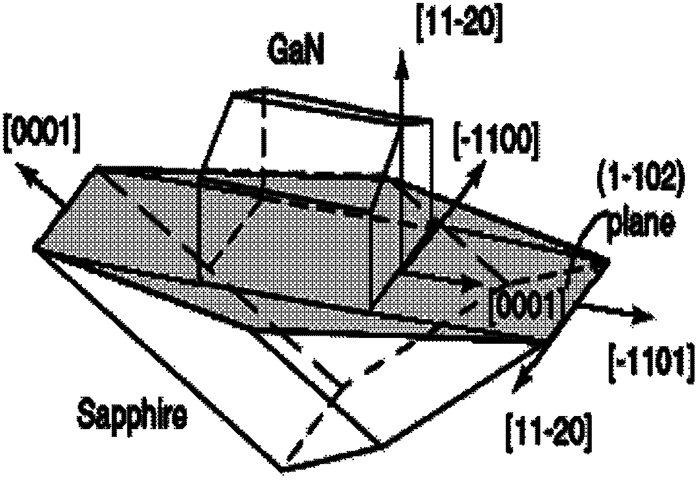
Raman characterization method of corrosion stress of alpha surface GaN epitaxial layer film
A technology of thin film corrosion and epitaxial layer, applied in the field of microelectronics, can solve the problems of epitaxial layer thin film stress error, unable to eliminate phonon peak shift, complicated means, etc., achieve simple formula, avoid formula derivation and mathematical calculation, and be easy to implement Effect
- Summary
- Abstract
- Description
- Claims
- Application Information
AI Technical Summary
Problems solved by technology
Method used
Image

Examples
Embodiment 1
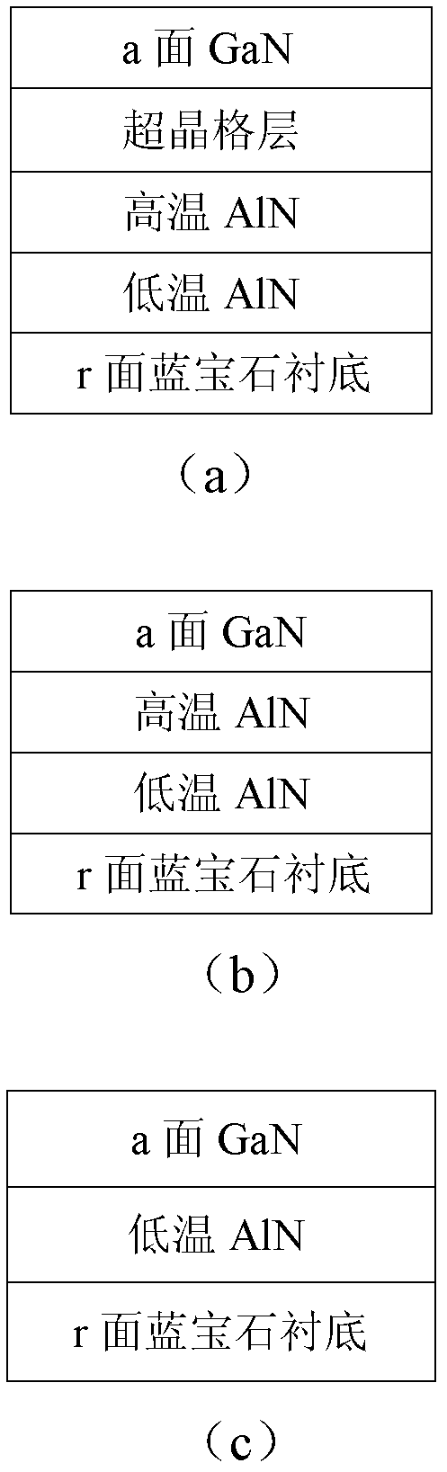
[0026] Example 1: for figure 2 Raman characterization of corrosion stress for the superlattice a-plane GaN sample shown in (a).
[0027] Step 1, performing surface cleaning treatment on the superlattice type a-plane GaN epitaxial film.
[0028] Place the superlattice a-plane GaN sample in a vacuum of 5.0×10 -3 mbar CVD furnace chamber, and a nitrogen gas flow rate of 60 liters per minute was introduced to remove scratches and surface attachments on the sample surface at room temperature.
[0029] In step 2, the superlattice type a-plane GaN epitaxial film sample from which surface pollutants have been removed is subjected to a Raman scattering test at room temperature using an argon ion laser with a wavelength of 514.5 nm.
[0030] Place the superlattice a-plane GaN epitaxial film sample on the Raman scattering test bench, and set the polarization mode of the Raman scattering instrument to For the a-plane GaN film, among the possible phonon vibration modes in this polariza...
Embodiment 2
[0044] Example 2: to figure 2 (b) Enhanced a-plane GaN samples shown in Raman characterization of corrosion stress.
[0045] Step 1, performing surface cleaning treatment on the enhanced a-plane GaN epitaxial film.
[0046] 1.1) Place the enhanced a-plane GaN sample in a vacuum of 5.0×10 -3 In a CVD furnace chamber of mbar; 1.2) Nitrogen gas with a flow rate of 80 liters per minute is fed into the CVD furnace chamber, and scratches and surface attachments on the surface of the film sample are removed at room temperature.
[0047] In step 2, the enhanced a-plane GaN epitaxial film sample from which surface pollutants have been removed is subjected to a Raman scattering test at room temperature using an argon ion laser with a wavelength of 514.5 nm.
[0048] Place the enhanced a-plane GaN epitaxial layer thin film sample on the Raman scattering test bench, and use an argon ion laser with a wavelength of 514.5 nm at room temperature to perform Raman on the enhanced a-plane GaN...
Embodiment 3
[0065] Example 3: to figure 2 (c) Raman characterization of corrosion stress for common a-plane GaN samples.
[0066]Step A, performing surface cleaning treatment on the ordinary a-plane GaN epitaxial film.
[0067] Place the normal a-plane GaN sample in a vacuum of 5.0×10 -3 mbar CVD furnace chamber, and a nitrogen gas flow rate of 100 liters per minute was introduced to remove scratches and surface attachments on the sample surface at room temperature.
PUM
| Property | Measurement | Unit |
|---|---|---|
| Wavelength | aaaaa | aaaaa |
Abstract
Description
Claims
Application Information