Supporting substrate, bonding substrate, method for manufacturing supporting substrate, and method for manufacturing bonding substrate

A technology of supporting substrate and manufacturing method, which is applied in the fields of supporting substrate, bonding substrate, manufacturing of supporting substrate and manufacturing of bonding substrate, can solve the problems of inability to obtain bonding strength, inability to be close to bonding surface, etc.

Inactive Publication Date: 2012-03-14
BRIDGESTONE CORP
View PDF5 Cites 2 Cited by
  • Summary
  • Abstract
  • Description
  • Claims
  • Application Information

AI Technical Summary

Problems solved by technology

Therefore, when bonding the support substrate to the single-crystal wafer, a gap is formed between the single-crystal wafer and the support substrate, and the bonded surfaces cannot be sufficiently approached, resulting in a problem that bonding strength cannot be obtained.

Method used


Image

  • Supporting substrate, bonding substrate, method for manufacturing supporting substrate, and method for manufacturing bonding substrate
  • Supporting substrate, bonding substrate, method for manufacturing supporting substrate, and method for manufacturing bonding substrate
  • Supporting substrate, bonding substrate, method for manufacturing supporting substrate, and method for manufacturing bonding substrate

Examples


Embodiment Construction

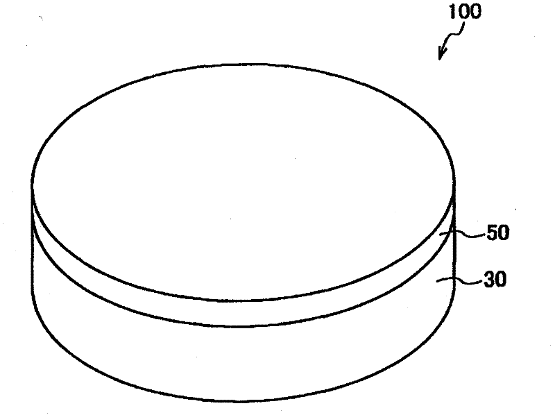
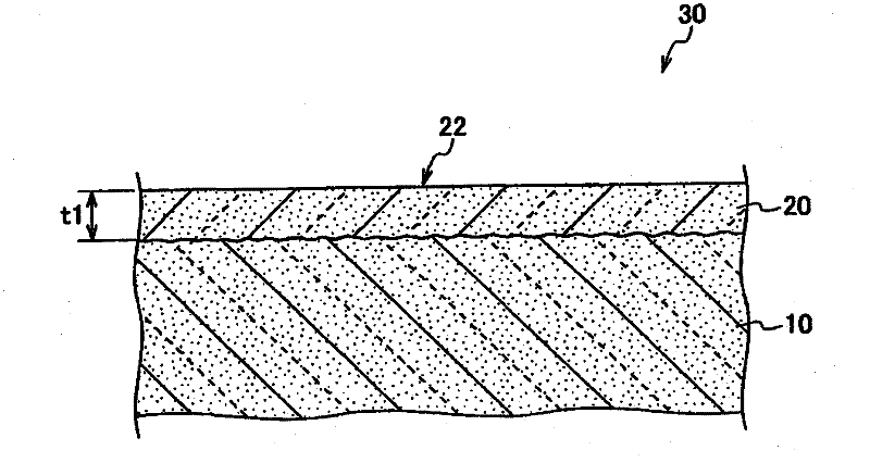
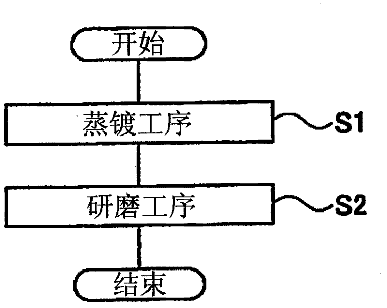
[0023] Next, the supporting substrate, the bonded substrate, the manufacturing method of the supporting substrate, and the manufacturing method of the bonded substrate of the present invention will be described with reference to the drawings. Specifically, (1) the overall structure of the bonded substrate, (2) the detailed structure of the supporting substrate, (3) the manufacturing method of the supporting substrate, (4) the manufacturing method of the bonded substrate, (5) comparative evaluation, ( 6) Action-Effect, (7) Other embodiments will be described.

[0024] In addition, in the following description of drawings, the same code|symbol is attached|subjected to the same part. However, the drawings are schematic diagrams, and it should be noted that ratios of dimensions and the like may differ from actual ratios of dimensions.

[0025] Therefore, specific dimensions and the like should be judged with reference to the following description. In addition, of course, the par...


PUM

PropertyMeasurementUnit
surface roughnessaaaaaaaaaa
thicknessaaaaaaaaaa
thicknessaaaaaaaaaa

Abstract

Provided is a supporting substrate (30) to be bonded on a single crystal wafer composed of a single crystal body. The supporting substrate is provided with a silicon carbide polycrystal substrate (10) composed of a silicon carbide polycrystal body, and a coat layer (20) deposited on the silicon carbide polycrystal substrate (10). The coat layer (20) is composed of silicon carbide or silicon and is in contact with the single crystal wafer, and the arithmetic average roughness of the contact surface (22) of the coat layer (20) in contact with the single crystal wafer is 1 nm or less.

Description

technical field [0001] The present invention relates to a bonded substrate including a single crystal wafer made of a single crystal and a support substrate bonded to the single crystal wafer, a support substrate constituting the bonded substrate, a method for manufacturing the support substrate, and a bonded substrate method. Background technique [0002] Conventionally, it has been found that single crystals such as silicon, silicon carbide, potassium nitride, and aluminum nitride not only have excellent heat resistance and voltage resistance, but also have excellent high-frequency characteristics. Therefore, as a semiconductor material used in next-generation LED devices, power devices, high-frequency devices, etc., wafers composed of the above-mentioned single crystals (hereinafter, abbreviated as single crystal wafers as appropriate) are known (for example, Patent Document 1 ). [0003] On the other hand, the above-mentioned single-crystal wafer has excellent characte...

Claims


Application Information

Patent Timeline
Patent Type & Authority Applications(China)
IPC IPC(8): C30B29/06C30B29/36
CPCC30B23/00C30B25/00C30B29/36C30B33/06C30B29/06
Inventor 牛田和宏
Owner BRIDGESTONE CORP
Why Eureka
Try Eureka