Devices formed from a non-polar plane of a crystalline material and method of making the same

A manufacturing method and technology of crystal materials, applied in semiconductor/solid-state device manufacturing, semiconductor devices, polycrystalline material growth, etc., can solve problems such as difficulties in gallium nitride semiconductor wafers

Active Publication Date: 2012-03-14
TAIWAN SEMICON MFG CO LTD
View PDF4 Cites 5 Cited by
  • Summary
  • Abstract
  • Description
  • Claims
  • Application Information

AI Technical Summary

Problems solved by technology

However, growing GaN semiconductor wafers

Method used


Image

  • Devices formed from a non-polar plane of a crystalline material and method of making the same
  • Devices formed from a non-polar plane of a crystalline material and method of making the same
  • Devices formed from a non-polar plane of a crystalline material and method of making the same

Examples


Embodiment Construction

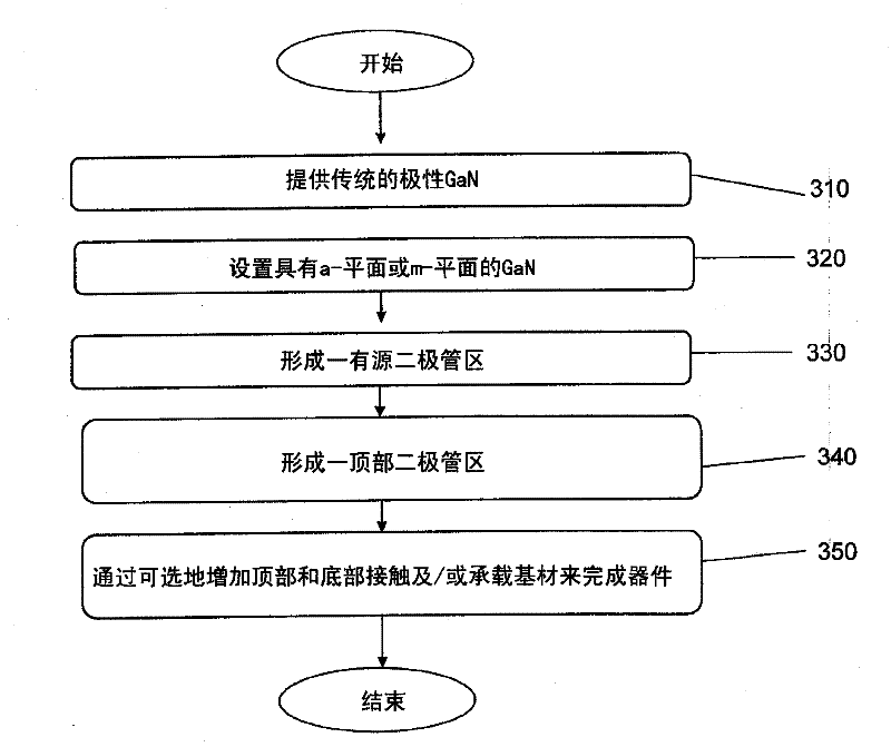
[0029] Embodiments of the inventive concept will be described in detail below and various examples are shown in the drawings, wherein like reference numerals are used for like parts throughout. The embodiments described below are described by referring to the figures in order to explain the concept of the present invention.

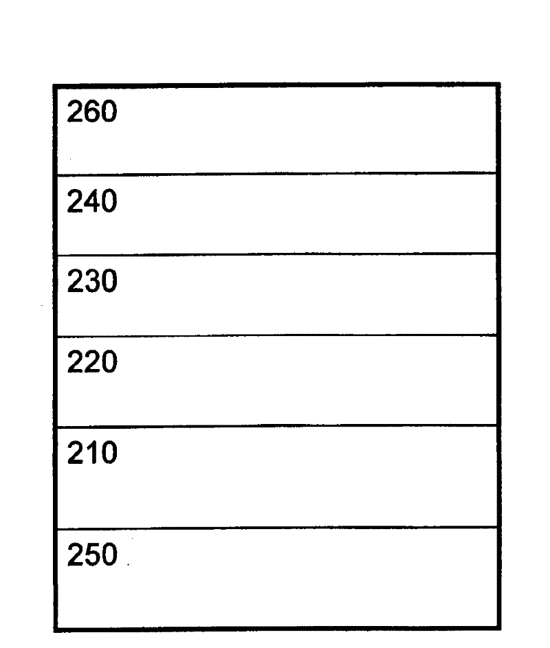
[0030] See figure 2 , a diode may include: a bottom diode region 220, an active diode region 230, and a top diode region 240, a first electrical contact 260 at the top of the device, and a second electrical contact 250 at the bottom of the device . Each zone 220, 230, 240 may comprise multiple layers. The diode can be coupled to a substrate 210 . Such as figure 2 As shown, in one embodiment, substrate 210 may be coupled between bottom contact 250 and active diode region 230 . Although figure 2 A vertical diode structure is shown, however it should be emphasized that the present invention is not limited to this structural arrangement and that othe...


PUM


Abstract

Materials, methods, structures and device including the same can provide a semiconductor device such as an LED using an active diode region corresponding to a non-polar face or surface of III-V semiconductor crystalline material. In some embodiments, an active diode region contains more non-polar III-V material oriented to a non-polar plane than III-V material oriented to a polar plane. In other embodiments, a bottom diode region contains more non-polar m-plane or a-plane surface area GaN than polar c-plane surface area GaN facing an active diode region.

Description

[0001] This application requires U.S. Provisional Application No. 61 / 166,184, filed on April 2, 2009, entitled "DEVICE FORMED FROM A NON-POLAR PLANE OF A CRYSTALLING MATERIAL AND METHOD OF MAKING THE SAME)", which is hereby incorporated by reference in its entirety. technical field [0002] The present invention relates to devices formed from a non-polar plane of a crystalline material, such as a non-polar plane of a III-N crystalline material, and methods of making the same. One embodiment relates to a non-polar light-emitting diode or method of making the same, or in particular to a non-polar light-emitting diode made from a III-nitride semiconductor material and a method of making the same. Background technique [0003] This section provides background information and presents information related to various aspects of the present invention that are described and / or claimed below and are not admitted to be prior art. [0004] Gallium nitride (GaN), and its ternary and qua...

Claims


Application Information

Patent Timeline
IPC IPC(8): H01L31/12
CPCH01L21/0243H01L21/02458H01L21/02494H01L21/0254H01L31/0304H01L33/007H01L33/08H01L33/12H01L33/16H01L33/24Y02E10/544Y02P70/50H01L31/12C30B29/406H01L21/02609H01L27/0814H01L29/045H01L29/2003H01L29/861
Inventor 安东尼·J·罗特费尔德
Owner TAIWAN SEMICON MFG CO LTD
Why Eureka
Try Eureka