Method for manufacturing structure of semiconductor device for forming structure of dual damascene
A device structure and semiconductor technology, which is applied in semiconductor/solid-state device manufacturing, electrical components, circuits, etc., can solve problems such as voids, poor trench profile, and overall electrical performance deterioration of semiconductor devices
- Summary
- Abstract
- Description
- Claims
- Application Information
AI Technical Summary
Problems solved by technology
Method used
Image

Examples
no. 1 example
[0050] Below, will refer to Figures 2A to 2H as well as image 3 The method for fabricating a double damascene structure according to the first embodiment of the present invention will be described in detail.
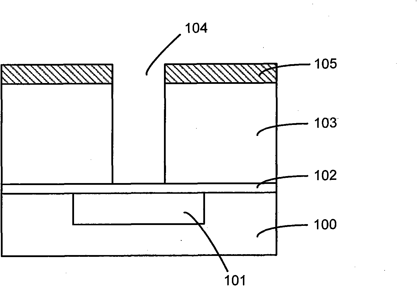
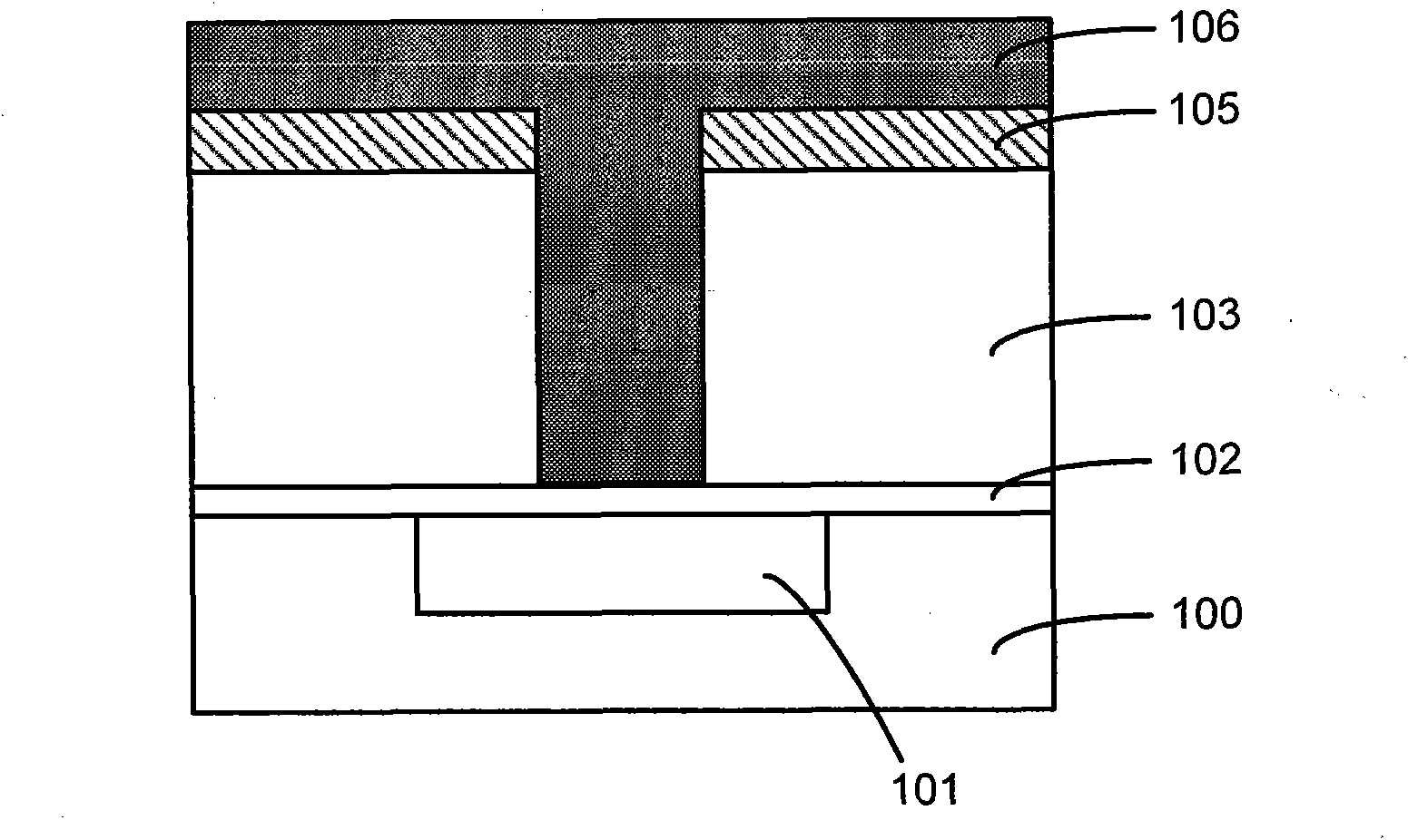
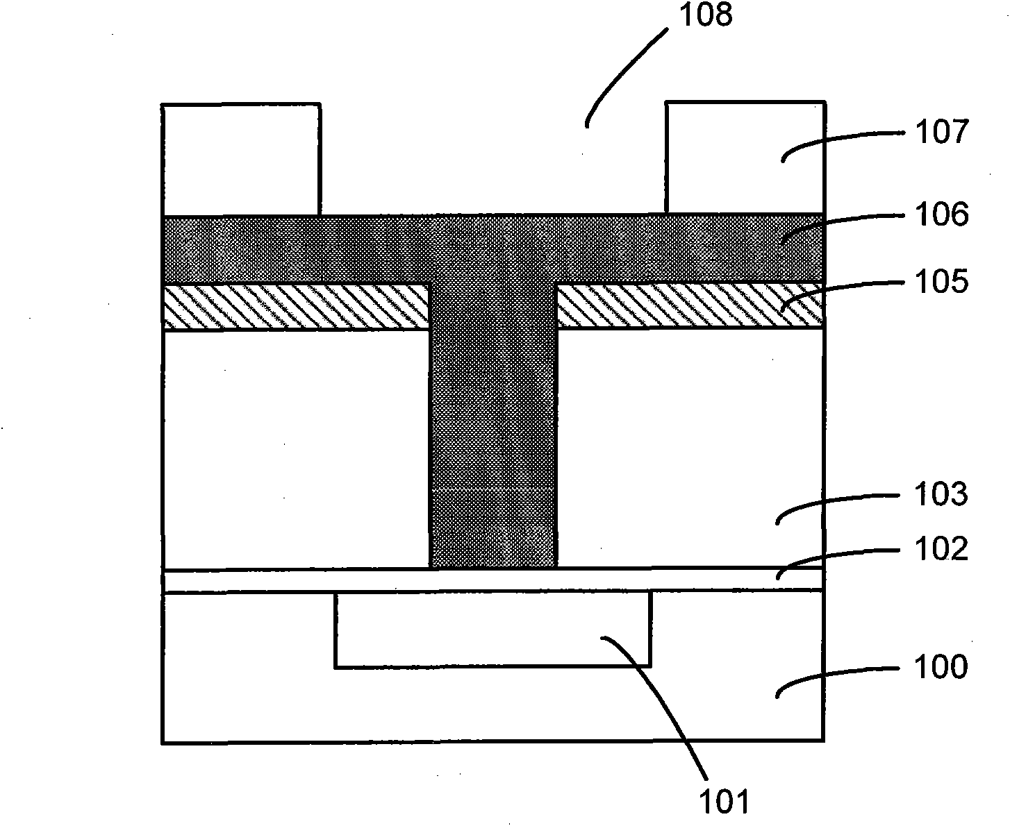
[0051] refer to Figures 2A to 2H ,in, Figures 2A to 2F A schematic cross-sectional view showing a method for fabricating a semiconductor device structure for forming a double damascene structure according to a first embodiment of the present invention. In this embodiment, a trench-first scheme is adopted.
[0052] First, if Figure 2A As shown in , a front-end device structure is provided, and an etch stop layer 202 and an IMD 210 are sequentially formed on the surface of the front-end device structure. Wherein, the front-end device structure may include, for example, a semiconductor substrate (not shown in the figure). Active source / drain regions, isolation grooves, field oxide layers, etc. have been formed in the semiconductor substrate, and a layer of undope...
no. 2 example
[0080] Below, will refer to Figures 4A to 4H as well as Figure 5 A method for fabricating a double damascene structure according to the second embodiment of the present invention will be described in detail.
[0081] refer to Figures 4A to 4H ,in, Figures 4A to 4F A schematic cross-sectional view showing a method for fabricating a semiconductor device structure for forming a double damascene structure according to a second embodiment of the present invention. It should be noted that the difference between this embodiment and the first embodiment is that it adopts a via-first solution.
[0082] First, if Figure 4A As shown in , a front-end device structure is provided, and an etch stop layer 402 and an IMD 410 are sequentially formed on the surface of the front-end device structure. Wherein, the front-end device structure may include, for example, a semiconductor substrate (not shown in the figure). Active source / drain regions, isolation grooves, field oxide layers, ...
PUM
| Property | Measurement | Unit |
|---|---|---|
| thickness | aaaaa | aaaaa |
| thickness | aaaaa | aaaaa |
| thickness | aaaaa | aaaaa |
Abstract
Description
Claims
Application Information
 - R&D
- Intellectual Property
- Life Sciences
- Materials
- Tech Scout
- Unparalleled Data Quality
- Higher Quality Content
- 60% Fewer Hallucinations
Browse by: Latest US Patents, China's latest patents, Technical Efficacy Thesaurus, Application Domain, Technology Topic, Popular Technical Reports.
© 2025 PatSnap. All rights reserved.Legal|Privacy policy|Modern Slavery Act Transparency Statement|Sitemap|About US| Contact US: help@patsnap.com