CMOS (complementary metal oxide semiconductor) device capable of reducing charge collection generated by radiation and preparation method thereof

A charge collection and device technology, applied in the field of CMOS devices, can solve problems such as aggravating the failure of single-event integrated circuits and output errors

Active Publication Date: 2012-03-21
PEKING UNIV
View PDF4 Cites 6 Cited by
  • Summary
  • Abstract
  • Description
  • Claims
  • Application Information

AI Technical Summary

Problems solved by technology

If a single event transient occurs at the output stage of a circuit, it will cause an error in the output; if it occurs in a memory element, it will cause the storage content to flip; even in a logic circuit, a single event will propagate along the logic circuit and during the propagation process The broadening effect appears in the medium, aggravating the probability of single event causing integrated circuit failure

Method used


Image

  • CMOS (complementary metal oxide semiconductor) device capable of reducing charge collection generated by radiation and preparation method thereof
  • CMOS (complementary metal oxide semiconductor) device capable of reducing charge collection generated by radiation and preparation method thereof
  • CMOS (complementary metal oxide semiconductor) device capable of reducing charge collection generated by radiation and preparation method thereof

Examples


Embodiment Construction

[0029] Embodiments of the present invention will be described in detail below in conjunction with the accompanying drawings.

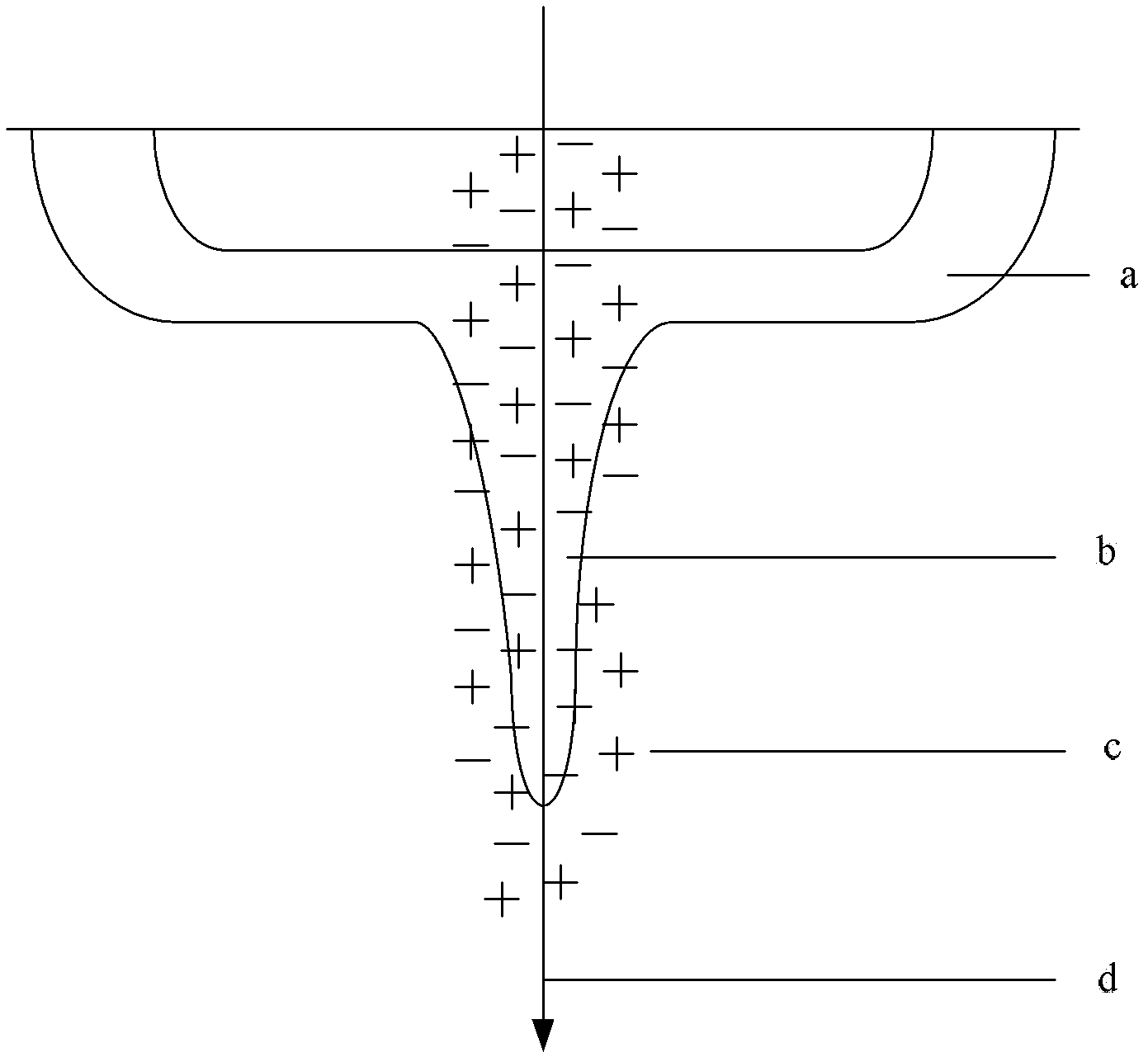
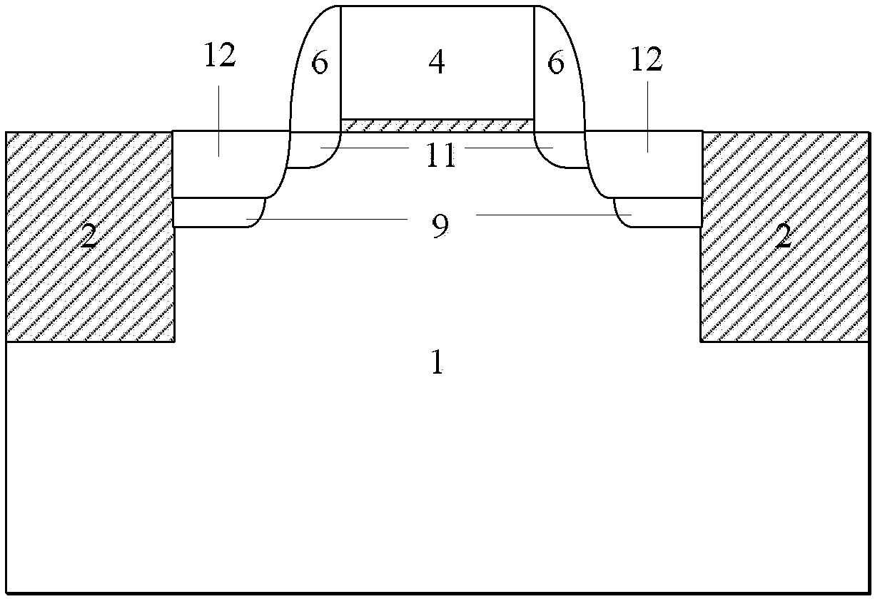
[0030] figure 2 For the cross-sectional view of the CMOS device proposed by the present invention, as shown in the figure, the CMOS device of the present invention includes a substrate 1, a device isolation region 2, a gate region 4, a gate spacer 6, a source region and a drain region 12, and an LDD region 11 , wherein the suppression charge collection region 9 is added directly below the source region and the drain region.

[0031] The specific implementation manner of the present invention will be described below by taking NMOS as an example.

[0032] 1) Substrate preparation: Lightly doped P-type silicon with a crystal orientation of (100) is used as the substrate 1, and the doping concentration is 10 15 ~10 16 cm -3 ;

[0033] 2) Formation of the device isolation region: Thermally grow a layer of silicon dioxide on the substrate 1 as a buffer...


PUM


Abstract

The invention discloses a CMOS (complementary metal oxide semiconductor) device capable of reducing charge collection generated by radiation and a preparation method thereof. The CMOS device provided by the invention is provided with a heavily doped charge restriction collecting region vertically below a source region and a drain region, the doping type of the charge restriction collecting region is opposite to those of the source region and the drain region, and the doping concentration is greater than or equal to those of the source region and the drain source. The transverse range of the charge restriction collecting region is slightly less than or equal to those of the source region and the drain region, and the transverse position of a channel is not more than the edges of the source region and the drain region. The CMOS device provided by the invention can greatly decrease the 'hopper' range generated under the action of independent particles so that the instantaneously collected charge can be decreased under the action of the electric field. As the width of a depletion layer is narrowed, an electron hole in the 'hopper' range is more difficult to diffuse to the edge of the depletion layer, thus the charge collected by a sensitive node can be greatly reduced and the influence of the transient independent particles on the integrated circuit can be effectively restrained.

Description

technical field [0001] The invention relates to a CMOS device, in particular to a CMOS device which reduces charge collection caused by radiation and a preparation method thereof. Background technique [0002] With the development of science and technology, more and more electronic systems need to be applied in various radiation environments, such as space radiation environment, nuclear radiation environment, simulated source environment and ground radiation environment. Various radiation effects can cause the failure of the performance of integrated circuits, and the single event effect has become the most important threat to the failure of thin gate oxide devices. The single event effect refers to that when high-energy charged particles in the radiation environment pass through the sensitive area of ​​integrated circuit components, a large number of electron-hole pairs deposited in the track are collected under the electric field of the depletion layer of the semiconductor...

Claims


Application Information

Patent Timeline
Patent Type & Authority Applications(China)
IPC IPC(8): H01L27/092H01L29/08H01L21/8238
CPCH01L29/7833H01L21/823814H01L29/1083H01L29/6653H01L21/8238H01L29/6656H01L29/6659
Inventor 黄如谭斐安霞黄芊芊杨东张兴
Owner PEKING UNIV
Why Eureka
Try Eureka